
EasyEDA PCB Design: Free Tool for Beginners Tutorial
If you have been wanting to design your own printed circuit board but thought it required expensive software and years of training, think again. EasyEDA PCB design is a free tool for beginners that runs entirely in your web browser — no installation needed. Developed by JLCPCB’s parent company, EasyEDA (now also available as EasyEDA Pro) supports schematic capture, PCB layout, simulation, and one-click ordering of your finished board. Thousands of Indian students, hobbyists, and startup engineers use EasyEDA every day to bring their circuit ideas to life. This step-by-step tutorial covers everything from creating a new project to generating Gerber files for manufacturing.
Getting Started with EasyEDA
EasyEDA Standard is available at easyeda.com. Create a free account using your email or Google login. The free tier gives you unlimited public projects; private projects require a (very affordable) paid plan. The browser-based editor supports Chrome, Firefox, and Edge — Chrome gives the best performance.
EasyEDA Standard vs EasyEDA Pro: EasyEDA Standard is the classic version best for beginners. EasyEDA Pro (downloadable desktop app) adds advanced features like hierarchical schematics, multi-board design, and differential pair routing — useful once you outgrow the basics. Start with Standard.
After logging in, click New Project. Give it a meaningful name (e.g., “555-LED-Blinker”). The project contains your schematic file (.sch) and PCB file (.pcb). You can have multiple schematics and PCBs in one project.
Creating Your Schematic
The schematic is your circuit diagram — it defines the electrical connections between components but has no physical dimensions. Think of it as the blueprint; the PCB layout is the actual construction.
Placing Components (Parts)
Press P (or click Place → Component) to open the parts library search. EasyEDA has a massive library of over 700,000 components with associated footprints — ideal for beginners who do not yet know how to create custom footprints.
Search for common parts:
- “NE555” — the classic 555 timer IC
- “BC547” — NPN BJT transistor
- “LM7805” — 5V voltage regulator
- “LED” — generic LED component
- Resistors: just type “R” and select a generic resistor, setting the value in the properties panel
- Capacitors: type “C” for generic capacitor
After placing all components on the schematic canvas, connect them using wires (W key). Click on a component pin, drag to the other pin, and click to complete the wire. Where wires cross without connecting, they automatically draw without a junction dot. To indicate a connection at a crossing, add a Junction (J key).
Adding Power Symbols and Net Labels
Use Power symbols (VCC, GND, +5V) from the library to avoid routing long wires across the schematic. Any two pins connected to the same power symbol or net label are electrically connected. This keeps your schematic clean and readable.
Annotation and Bill of Materials
Assign reference designators (R1, R2, C1, U1, etc.) automatically: go to Tools → Auto Annotate. Then fill in the Value field for each component (10k, 100n, NE555, etc.) in the Properties panel. This information flows through to your Bill of Materials (BOM) and Gerber files.
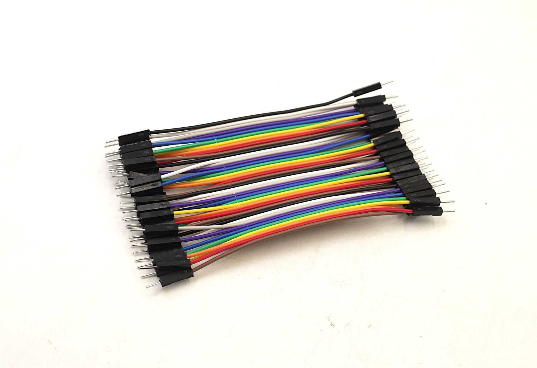
10CM Male To Male Breadboard Jumper Wires – 40Pcs
Prototype and verify your EasyEDA design on a breadboard before sending it for PCB fabrication. These 2.54 mm pitch wires are perfect for the job.
Converting to PCB Layout
Once your schematic is complete and error-free, generate the PCB layout by clicking Design → Convert to PCB (or press the PCB icon in the toolbar). EasyEDA creates a new PCB document and imports all components with their footprints. The components appear as a jumbled pile with thin blue lines (called ratsnest lines or airwires) connecting pins that need to be electrically connected by copper traces.
Before laying out your PCB, set the board outline in the Border layer. Draw a rectangle or custom shape that defines the physical size of your PCB. Standard affordable sizes from JLCPCB start at 100×100 mm for as little as $2 USD for 5 boards — extremely economical for Indian makers.
PCB Layout: Placing Components and Routing Traces
Component Placement Strategy
Good placement is 70% of good PCB design. Follow these principles:
- Group related components: Keep decoupling capacitors (100 nF) right next to IC power pins — within 2–3 mm is ideal
- Minimise ratsnest crossing: Rotate and arrange components so airwires overlap as little as possible. The fewer crossings, the easier routing will be
- Respect connector placement: Power connectors, USB ports, and headers should be at the board edge for easy access
- Heat-generating components: Place voltage regulators, MOSFETs, and power resistors where airflow is available. Avoid placing them under heatsink-mounted components
- High-speed signals short: Keep oscillator, crystal, and clock traces as short as possible to reduce EMI
Routing Traces
Select the Route Tracks tool (X key). Click on a pad, then click to set waypoints, and click the destination pad to complete the connection. EasyEDA turns completed traces red (Top copper) or blue (Bottom copper), and the corresponding ratsnest line disappears.
Set trace width before routing: click the trace width dropdown in the toolbar or go to Design → Net Inspector to set width rules per net. Use:
- 0.3–0.5 mm for signal traces (I²C, SPI, GPIO)
- 0.8–1.5 mm for moderate power (100 mA – 1 A)
- 2–4 mm for high-current power rails (3 A+)
Two-Layer Routing
EasyEDA Standard supports 2-layer PCBs (top and bottom copper). Use vias (V key) to switch between layers when a trace cannot be routed without crossing another. Vias add cost (every hole is drilled), so minimise via count. A common strategy is to route all horizontal traces on top and all vertical traces on bottom — this naturally reduces via count.
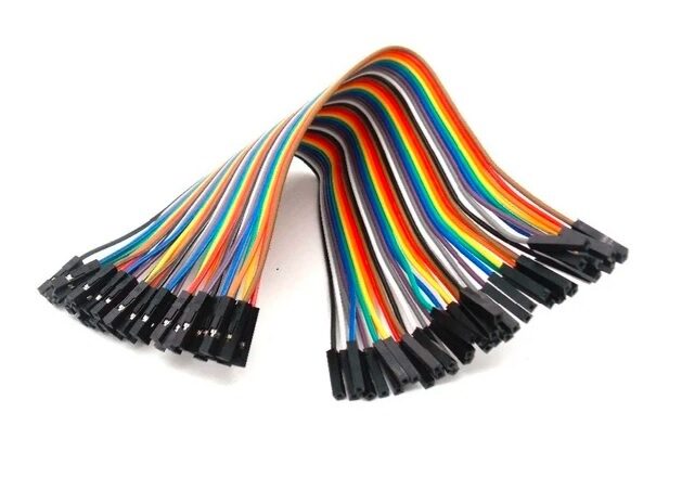
10CM Female To Female Breadboard Jumper Wires – 40Pcs
Connect Arduino, sensors, and your prototype circuits before you finalise your EasyEDA layout. Female-to-female wires work with standard pin headers.
Design Rule Check (DRC) and Copper Pour
Copper Pour (Ground Plane)
Before running DRC, add a copper pour for your ground net. Select the Copper Area tool (Shift+M), draw a polygon around your entire board area on the Bottom copper layer, and set it to the GND net. EasyEDA fills the area with copper, connecting all GND pads automatically. This creates a ground plane that:
- Provides a low-impedance return path for all signals
- Acts as a thermal spreader
- Reduces EMI by shielding signals from the ground plane reference
- Eliminates the need to route most GND connections manually
Running DRC
Go to Design → Design Rule Check. DRC checks for:
- Clearance violations (traces too close to each other or to board edge)
- Unconnected nets (ratsnest lines remaining — these are missing connections!)
- Pad clearance issues
- Drill size violations
Fix every error before exporting Gerber files. Unconnected nets are circuit faults — the PCB will not work as designed. Clearance violations may cause shorts during manufacturing.
Generating Gerber Files and Ordering
Gerber is the industry-standard file format for PCB manufacturing. Go to Fabrication → PCB Fabrication File (Gerber). EasyEDA generates a ZIP file containing all Gerber layers (copper, solder mask, silkscreen, drill files). Download this ZIP.
For Indian makers ordering from JLCPCB: the “Order on JLCPCB” button in EasyEDA directly uploads your design to JLCPCB’s quoting system. 5 boards (100×100 mm, 2-layer, 1.6 mm FR4, green solder mask) typically cost around $2 USD + shipping to India (approximately ₹200–500 depending on the courier option chosen). Delivery takes 10–20 days with economy shipping.
Indian PCB vendors like PCBPower (Ahmedabad), Satvik Circuits, or local manufacturers offer faster delivery if needed. Most accept standard Gerber ZIP files.
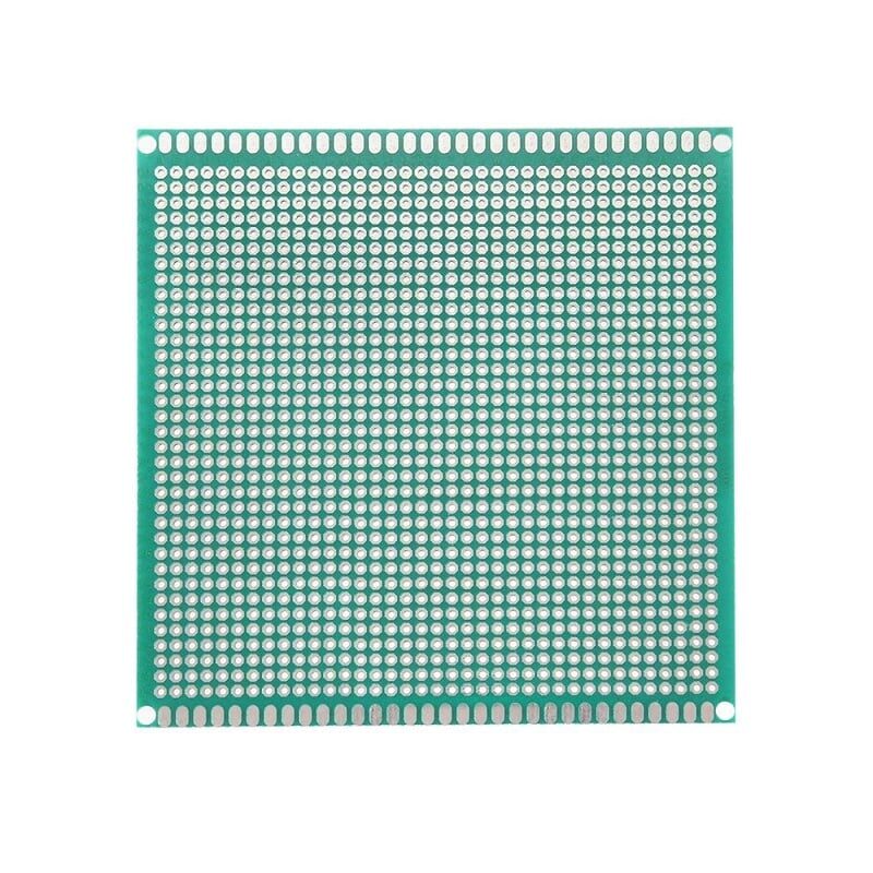
10×10 cm Universal PCB Prototype Board
While you wait for your custom PCB order, build and test your design on this universal prototype board. Single-sided, 2.54 mm pitch — matches standard DIP IC spacing.
Pro Tips for Better PCB Designs
Always prototype on breadboard first: Before committing to a PCB, build and test the circuit on a breadboard using jumper wires. Changing a schematic in EasyEDA is easy; changing a fabricated PCB is impossible.
Add test points: Place small circular pads (1–2 mm diameter, labelled TP1, TP2, etc.) on critical signals. Test points let you probe the board with a multimeter or oscilloscope probe without needing to touch component pins.
Label everything in silkscreen: Use the Silkscreen layer to label connectors (PIN1 marker, J1, J2), test points, and jumper settings. Good silkscreen annotation saves hours of debugging later.
Check your footprints with real components: Before ordering, print the PCB layout at 1:1 scale on paper and place physical components on top. This quickly reveals footprint errors — wrong pad spacing, wrong package size — that are expensive to discover on a fabricated board.
Save revisions: EasyEDA saves automatically, but use the Git-like version history (right-click project → History) to tag important milestones. Label them “v1-breadboard-verified” or “v2-added-USB” for clarity.
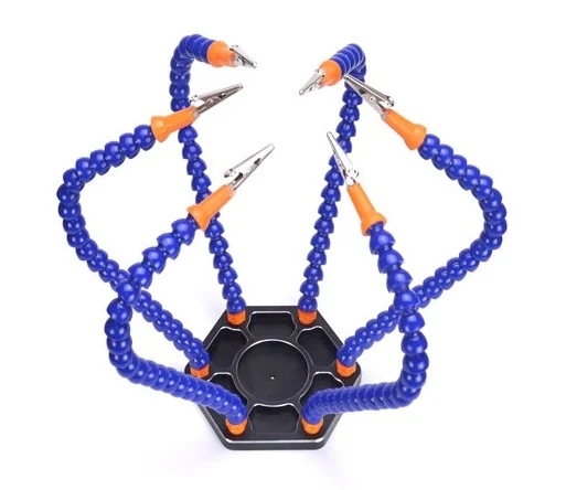
6 Flexible Arms Soldering Station with Alligator Clips
Once your custom PCB arrives, assemble it comfortably with this six-arm helping hand station. Swivelling alligator clips hold your board and components at any angle.
Frequently Asked Questions
Is EasyEDA completely free to use?
Yes, EasyEDA Standard is free with unlimited public projects. Private projects (visible only to you) require a paid subscription. For students and hobbyists sharing open-source designs, the free plan is sufficient. EasyEDA Pro (desktop application) also has a free personal tier with some limitations.
Can I design a 4-layer PCB in EasyEDA for free?
EasyEDA Standard supports 2-layer PCBs for free. EasyEDA Pro supports multi-layer (4-layer and above) PCB design. Most beginner and intermediate designs work well with 2 layers. If you need 4 layers (for high-speed designs, dense routing, or separate power/ground planes), upgrading to EasyEDA Pro or switching to KiCad (fully free, open-source) is the next step.
What is the difference between schematic and PCB layout?
The schematic shows logical connections between component pins — it tells you what is connected to what. The PCB layout shows physical positions of components and actual copper traces on the board — it tells you where everything is physically located. Both must agree: every connection in the schematic must have a corresponding copper trace in the PCB layout.
How long does it take to learn EasyEDA as a complete beginner?
Most beginners can design their first simple schematic and PCB within 2–4 hours of starting. Watch EasyEDA’s official YouTube tutorials and the many Indian educator videos available. Expect a learning curve of 2–4 weeks for comfortable proficiency and a few months to design complex boards confidently.
Can I use EasyEDA libraries with KiCad?
EasyEDA components can be exported as KiCad footprint files (.kicad_mod). Several third-party tools convert EasyEDA JSON library exports to KiCad format. The easyeda2kicad Python package is popular for this purpose. However, many EasyEDA users simply stick with EasyEDA for its seamless JLCPCB integration.
Design Your First PCB Today
EasyEDA makes PCB design accessible to every Indian maker and student. Once your board arrives, you will need quality components to populate it. Shop resistors, capacitors, transistors, ICs, jumper wires, prototype boards, and soldering tools at Zbotic — with fast delivery across India.


Add comment