


Description:
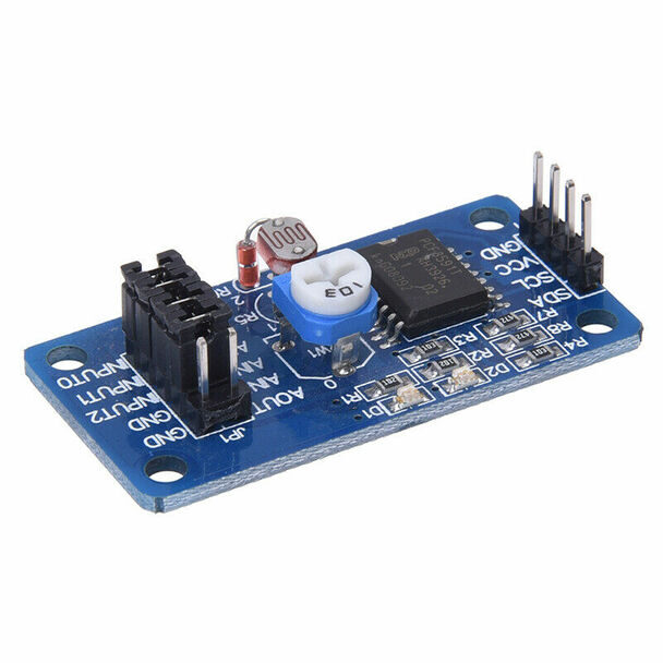
PCF8591 Module Analog to Digital / Digital-Analog Converter Module
This is a breakout/prototype board designed for the PCF8591 IC. The PCF8591 is a low-power, 8-bit CMOS data acquisition device that operates on a single supply. It features four analog inputs, one analog output, and a serial I²C-bus interface for easy communication.
The module includes three address pins—A0, A1, and A2—which allow you to set the hardware address, enabling the connection of up to eight devices on the same I²C bus without the need for additional hardware. Data transfer to and from the device is done serially via the bidirectional I²C bus.
The PCF8591 offers key features such as analog input multiplexing, an on-chip track-and-hold function, 8-bit analog-to-digital conversion, and 8-bit digital-to-analog conversion. The maximum conversion rate is determined by the speed of the I²C bus.
PCF8591 IC Features:
- Single power supply
- A PCF8591 operating voltage range of 2.5V-6V
- Low standby current
- Via I2C bus serial input/output
- PCF8591 by 3 hardware address pins addressing
- PCF8591 I2C bus speed sampling rate decided
- 4 analog inputs programmable single-ended or differential input
- Automatic incremental channel selection
- PCF8591 analog voltage range from VSS to VDD
- PCF8591 built-in track-and-hold circuit
- 8-bit successive approximation A / D converter
- 1 analog output DAC gain
Module Features:
- The module supports external voltage input of the 4-way acquisition (voltage input range of 0-5v)
- The module integrated photoresistor by AD collection precise value of the ambient light intensity
- Module integrated thermistor by the precise value of the ambient temperature of the AD acquisition
- Module integrated 1 channel 0-5V voltage input acquisition (the blue potentiometer to adjust the input voltage)
- Modules with power indicator (for the module power supply indicator lights)
- Modules with DA output indicator, when the module DA output interface voltage reaches a certain value, will be lit panel the DA output indicator, the higher the voltage, the more obvious indicator brightness
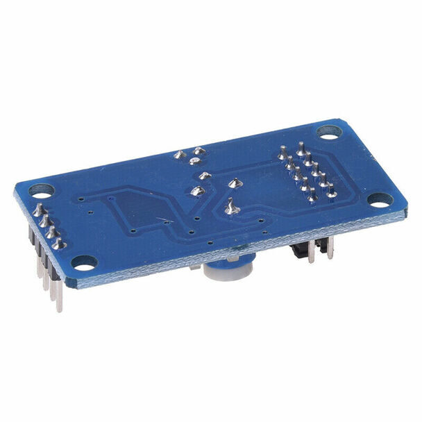
- Module PCB size: 3.6cm x 2.3cm
- A standard double panel, thickness 1.6mm, nice layout, surrounded by a through-hole, aperture: 3mm, convenient fixed.
Module interface specification:
The Left
- AOUT chip DA output interface
- AINO chip analog input interface 0
- AIN1 chip analog input interface 1
- AIN2 chip analog input interface 2
- AIN3 chip analog input interface 3
The Right
- SCL – IIC clock interface connected to microcontroller IO port
- SDA – IIC digital interface connected to microcontroller IO port
- GND – connected to ground
- VCC – connected to 3.3v-5v
Four red jumper-cap instruction
- P4 – connected to P4 shorting cap, select thermistor access circuit
- P5 – connect P5 shorting cap, select photoresistor access circuit
- P6 – connected to P6 shorting cap, select 0-5V adjustable voltage access circuit
Specifications:
| IC Chip | PCF8951 |
|---|---|
| Operating Voltage (VDC): | 2.5 ~ 6 |
| PCB Size ( L x W ) mm | 35 x 23 |
Package Includes
- 1 x PCF8591 Module (Analog to Digital / Digital-Analog Converter Module)
Attachments:
PCF8591 Datasheet
Technical Specifications
| Model | PCF8591 |
|---|---|
| SKU | AI0616 |
| Weight | 0.01 kg |
| Availability | In Stock |
Applications & Use Cases
The PCF8591 Module Analog to Digital / Digital-Analog Converter Module is a versatile audio amplifier module used across a wide range of applications including electronics projects, DIY builds, prototyping, and educational experiments.
Common use cases:
- Integrating into a custom electronics project
- Learning and experimenting with circuits
- Replacing or upgrading components in existing setups
This product is ideal for electronics enthusiasts, engineers, and students.
Technical Tip: Always verify voltage and current requirements before connecting to your circuit. Check datasheets for detailed specifications and pin configurations.
Shipping & Delivery
- Free shipping on orders above ₹999 across India
- Dispatched within 1-3 business days
- Expected delivery: 3-7 business days depending on location
- Secure packaging to ensure safe transit of electronic components


Raghav Mishra (verified owner) –
This PCF8591 Module Analog to Digital / performs flawlessly. Voltage regulation is precise and consistent.
Zubin Pandey (verified owner) –
Good quality PCF8591 Module Analog to Digital /. Ripple is low. Suitable for most electronics projects.
Kiara Bajaj –
Perfect PCF8591 Module Analog to Digital / for my portable project. Battery life is better than expected.
Gauri Saxena (verified owner) –
This PCF8591 Module Analog to Digital / is reliable and efficient. Running my IoT setup 24/7 with no issues.
Meera Sharma (verified owner) –
Bought multiple units of this PCF8591 Module Analog to Digital /. All consistent quality. Zbotic is reliable.
Rohit Grewal (verified owner) –
Okay PCF8591 Module Analog to Digital /. Output is slightly off from specified but within usable range.
Kabir Bhandari (verified owner) –
This PCF8591 Module Analog to Digital / is reliable and efficient. Running my IoT setup 24/7 with no issues.
Suresh Tandon (verified owner) –
Good PCF8591 Module Analog to Digital /. Output is stable. Gets slightly warm under full load but nothing concerning.
Anil Vyas (verified owner) –
Excellent PCF8591 Module Analog to Digital /! Output is stable and reliable. Perfect for my electronics project.
Aarav Mukherjee –
Perfect PCF8591 Module Analog to Digital / for my portable project. Battery life is better than expected.
Harshit Rao (verified owner) –
Good quality PCF8591 Module Analog to Digital /. Ripple is low. Suitable for most electronics projects.
Hardik Negi (verified owner) –
Decent PCF8591 Module Analog to Digital /. Voltage output is accurate. Compact form factor is a plus.
Mayank Naidu (verified owner) –
Average PCF8591 Module Analog to Digital /. Works but efficiency could be better. Adequate for basic projects.
Sachin Vyas (verified owner) –
Good PCF8591 Module Analog to Digital /. Output is stable. Gets slightly warm under full load but nothing concerning.
Lalit Grewal (verified owner) –
Excellent PCF8591 Module Analog to Digital /! Output is stable and reliable. Perfect for my electronics project.