
Instrumentation Amplifier INA128: Differential Signal Guide
The instrumentation amplifier INA128 is one of the most popular and versatile precision differential amplifiers in analog circuit design. Whether you’re amplifying the tiny signal from a Wheatstone bridge pressure sensor, reading a thermocouple in a temperature controller, or building a portable ECG monitor, the INA128 provides the high common-mode rejection, low noise, and single-resistor gain setting that makes it indispensable for sensor interface circuits. This guide covers everything Indian makers and engineers need to know about using the INA128 effectively.
What Is the INA128 and Why Use It?
An instrumentation amplifier (in-amp) is a specialized differential amplifier designed for high-accuracy, low-noise amplification of small differential signals in the presence of large common-mode voltages. Unlike a standard op-amp used as a difference amplifier (which requires precisely matched external resistors), an instrumentation amplifier has all resistors internally matched at the factory — achieving high CMRR without requiring tight external tolerances.
The INA128 from Texas Instruments is an industry-standard precision in-amp featuring:
- Gain range: 1 to 10,000 (set by a single external resistor RG)
- CMRR: 120dB minimum at G=1000
- Input offset voltage: 25µV maximum
- Input bias current: 5nA maximum
- Input noise: 8nV/√Hz at 1kHz
- Bandwidth: 200kHz at G=100
- Supply range: ±2.25V to ±18V
- Package: 8-pin DIP or SOP
The INA128 is functionally equivalent to the INA128P (plastic DIP package) and INA128U (SOIC-8 package). The INA129 is a pin-compatible alternative with slightly different specifications. Both are manufactured by Texas Instruments and widely available in India from distributors like Mouser India, Digikey, and local electronics shops at ₹100–250 per IC.
Internal Architecture: Three Op-Amp Topology
The INA128 uses the classic three-op-amp instrumentation amplifier topology that provides several important advantages over simpler two-op-amp or single-op-amp difference amplifier configurations.
Stage 1: Input Buffer Amplifiers
Two op-amps in the first stage buffer the differential inputs. Each input connects to the non-inverting input of one op-amp. The gain-setting resistor RG connects between the output of both first-stage op-amps through internal 24.7kΩ resistors. This configuration provides:
- Very high input impedance (typically 10GΩ || 2pF) — doesn’t load the source
- Equal gain on both inputs — ensures high CMRR
- Common-mode signals (appearing equally on both inputs) are passed with unity gain through the first stage
- Differential signals are amplified with gain = 1 + 2×(24.7kΩ / RG)
Stage 2: Difference Amplifier
The second stage is a precision difference amplifier with all resistors internally laser-trimmed to 10ppm matching. It subtracts the two first-stage outputs to reject the common-mode component and amplify the differential component with unity gain. The VREF pin connects to the second stage’s reference input, allowing the output to be offset — useful for single-supply operation.
Total Gain Formula
G = 1 + 50kΩ / RG
(where 50kΩ is the sum of two internal 24.7kΩ ≈ 25kΩ resistors, slightly simplified in the datasheet)
Note: Texas Instruments specifies the gain formula as G = 1 + (50kΩ / RG) in the INA128 datasheet. The actual internal resistor values are trimmed such that this formula is accurate to within the gain error specification.
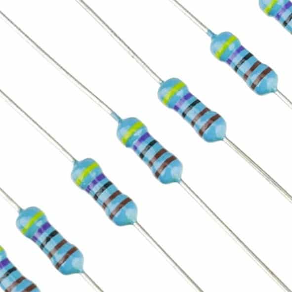
1.5 Ohm 1/4W Metal Film Resistor MFR (Pack of 100)
1% tolerance metal film resistors for precise RG gain-setting in INA128 circuits. Better thermal stability and accuracy than carbon film types. Pack of 100.
Gain Setting with a Single Resistor
The gain of the INA128 is set by a single external resistor RG connected between pins 1 and 8. The gain formula is:
G = 1 + (50kΩ / RG)
Common Gain Settings
| Desired Gain | RG (calculated) | RG (nearest standard E96) | Actual Gain |
|---|---|---|---|
| 1 | ∞ (no resistor) | Open circuit | 1.00 |
| 10 | 5.556kΩ | 5.49kΩ | 10.1 |
| 100 | 505Ω | 499Ω | 101.2 |
| 1000 | 50.05Ω | 49.9Ω | 1002 |
Important: For high gains (G > 100), small tolerances in RG cause large percentage errors in gain. Use 0.1% or better resistors for RG when G > 100. A 1% error in RG at G=1000 gives approximately 1% gain error — 10mV error on a 1V full-scale output.
Variable Gain with Potentiometer
For applications requiring adjustable gain, connect a potentiometer in series with a small fixed resistor as RG. The fixed resistor sets the maximum gain (when pot is at minimum), preventing gain from going to infinity if the pot wiper loses contact. Example: 499Ω fixed + 5kΩ potentiometer gives G range of 11 to 101.
Key Electrical Specifications
Input Offset Voltage and Drift
The INA128’s 25µV maximum offset voltage (at room temperature) is one of its key selling points. For a G=100 circuit measuring a 0–100mV bridge signal, this 25µV referred-to-input offset creates only 2.5mV error at the output — acceptable for most applications. For lower offset, consider the INA128A (50µV max) or the INA129 (5µV max in grade P models).
The offset voltage temperature drift is 0.5µV/°C typical, 2µV/°C maximum — important for industrial equipment operating over India’s wide ambient temperature range (0–50°C typical for control panels).
CMRR vs Frequency
CMRR decreases with frequency due to mismatches in the internal resistor network becoming significant at higher frequencies. The INA128 maintains 80dB CMRR up to 10kHz at G=1. At G=100, CMRR is 100dB up to 1kHz. For 50Hz mains noise rejection, even G=1 CMRR of 110dB is excellent — attenuating 230V mains interference to under 2mV.
Single Supply Operation
The INA128 requires dual supplies (±VS). For single-supply operation, connect V– to GND and use VREF pin to set the output mid-rail (VREF = VS/2). Minimum supply is ±2.25V, so ±3V or ±5V from a charge pump or boost converter works well for battery-powered applications. The LM35 temperature sensor, for example, outputs 10mV/°C — a gain of 100 on the INA128 gives 1V/°C output, easily readable by a 10-bit ADC with 5V reference.

LM35 Temperature Sensors
Precision linear temperature sensor outputting 10mV/°C. Pair with INA128 for amplified temperature measurement with excellent noise rejection. No calibration needed.
Wheatstone Bridge Sensor Amplification
Wheatstone bridge sensors (pressure, strain gauge, load cell, RTD bridges) produce a differential output voltage of 1–10mV per volt of excitation. For a 5V excited bridge with 2mV/V sensitivity, the full-scale output is only 10mV — requiring significant amplification before it can be read by a microcontroller’s ADC.
Complete Bridge Amplifier Circuit
For a 350Ω full bridge (typical for commercial load cells):
- Excite the bridge with a stable 5V reference (use a precision voltage reference, NOT the MCU’s 3.3V supply)
- Connect bridge differential outputs to INA128 pins 2 (–IN) and 3 (+IN)
- Set RG for desired gain: G = 500 → RG = 50kΩ/499 = 100Ω (use 100.5Ω or 0–200Ω pot for calibration)
- Connect VREF (pin 5) to bridge excitation midpoint or to ADC reference midpoint for single-supply operation
- Output: 10mV × 500 = 5V full scale — perfect for a 5V ADC reference
The INA128’s high input impedance (10GΩ) means it doesn’t load the 350Ω bridge, avoiding measurement errors. Its 5nA input bias current creates only 1.75µV offset across the 350Ω source impedance — negligible.
Thermocouple Signal Conditioning
Type K thermocouples generate approximately 41µV/°C. To measure 0–500°C with a 10-bit ADC (0–5V range, 4.88mV/LSB), the required gain is:
G = 5V / (500°C × 41µV/°C) = 5V / 20.5mV = 244
RG = 50kΩ / (G–1) = 50kΩ / 243 = 205.8Ω → use 200Ω + 10Ω trimmer for calibration.
Cold junction compensation: Thermocouple output is referenced to the cold junction temperature. For accurate absolute temperature, measure the cold junction with an LM35 or NTC thermistor and add (or subtract via software) the cold junction temperature to the thermocouple reading. Dedicated ICs like the MAX31855 integrate this, but the INA128 + LM35 approach gives more flexibility and lower cost (₹150 total vs ₹300+ for MAX31855).
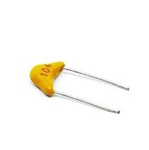
0.1/100nF Multilayer Ceramic Capacitor (Pack of 50)
Bypass capacitors for INA128 power supply pins — essential for keeping noise out of precision instrumentation amplifier circuits. Pack of 50.
PCB Layout and Decoupling Tips
Precision instrumentation amplifiers are sensitive to layout. A poor layout can degrade CMRR from 120dB to 60dB or worse.
Power Supply Decoupling
- Place 100nF ceramic capacitors from V+ to GND and V– to GND as close as possible to the INA128 supply pins (pins 7 and 4)
- Add 10µF tantalum or electrolytic capacitors 5–10mm away for low-frequency decoupling
- Power supply noise couples into the output as: Vnoise_out = Vsupply_noise / PSRR
- INA128 PSRR is typically 100dB — but only with adequate decoupling
Input Guard Rings
For high-impedance sources or long cable runs, PCB leakage currents across the amplifier’s input pins can create offset errors. A guard ring driven by the buffer amplifier output (the guard point) surrounds the input traces and reduces effective PCB leakage resistance from GΩ to TΩ range. Essential for sub-nA bias current measurements.
RG Placement
Place RG as close as possible to the INA128 pins 1 and 8. Long traces from RG to the IC act as antennas and add parasitic resistance that changes the gain. Keep RG leads under 5mm total length.
INA128 vs INA121 vs INA126: Which to Choose?
| Parameter | INA128 | INA121 | INA126 |
|---|---|---|---|
| Offset Voltage (max) | 25µV | 50µV | 150µV |
| Bias Current (max) | 5nA | 10pA (FET) | 15nA |
| Bandwidth (G=100) | 200kHz | 60kHz | 200kHz |
| Min Supply | ±2.25V | ±2.25V | ±1.35V (single 2.7V) |
| Best For | Bridge sensors, ECG | High-Z sources (pH, electrodes) | Battery-powered, cost |
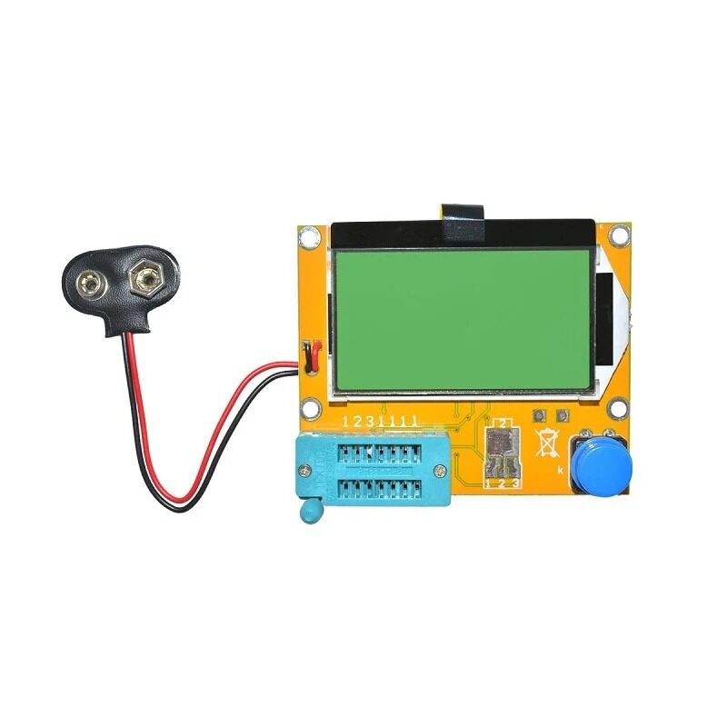
LCR-T4 LCD Graphical Component Tester
Verify your RG resistor values precisely before soldering into INA128 circuits. Measures resistance with 0.1Ω resolution. Essential for precision analog work.
Frequently Asked Questions
Can the INA128 work with a single 5V supply?
Yes, but with limitations. Connect V– to GND and V+ to 5V. The input common-mode range extends from V– + 1.9V to V+ – 1.7V, so inputs must stay between 1.9V and 3.3V. Connect VREF to 2.5V (from a voltage divider or precision reference) to centre the output. The output can swing from about 1.5V to 3.5V with 5V single supply — giving only about 2V of usable output range.
What is the maximum input voltage for the INA128?
The differential input voltage must not exceed ±40V for the INA128 (absolute maximum). The common-mode input voltage must stay within ±VS – 1.9V (input common-mode range). For sensing signals from 12V systems with a ±15V supply, the INA128 can handle common-mode inputs up to ±13.1V. For 48V or higher systems, add input protection resistors and voltage clamp diodes.
How does the INA128 compare to a standard op-amp difference amplifier?
A standard op-amp difference amplifier requires four external resistors matched to 0.01% for 80dB CMRR — expensive and difficult to achieve. The INA128 provides 120dB CMRR with no external matching required. The INA128 also has much higher input impedance (10GΩ vs typically 10–40kΩ for a discrete difference amp), which avoids loading the signal source.
Why does my INA128 circuit oscillate at high gains?
At high gains (G > 100), the INA128’s bandwidth is reduced and phase margin decreases. Adding capacitive loads (long output cables, ADC sample-hold capacitance) can cause oscillation. Add a 100Ω–1kΩ series resistor between the INA128 output and the load. Also ensure good decoupling capacitors (100nF + 10µF) on both supply pins.
What is the INA128’s noise performance for ECG applications?
For ECG (bandwidth 0.05–150Hz), the INA128’s 8nV/√Hz voltage noise and 50fA/√Hz current noise are excellent. The integrated noise over the ECG band (150Hz) is approximately 8nV × √150 ≈ 98nV RMS referred to input. With G=1000 gain, the output noise is 98µV RMS — well below the ECG amplitude of 1–5mV, providing a signal-to-noise ratio better than 30dB before digital filtering.
Building precision analog circuits? Zbotic stocks precision resistors, decoupling capacitors, temperature sensors, and all the components needed for instrumentation amplifier applications. Explore our Electronics Components range and get same-day dispatch on orders placed before 2 PM!


Add comment