
Decoupling Capacitor Placement: Best Practice for PCB Design
Among all the small details that separate a working PCB from a temperamental one, decoupling capacitor placement in PCB design stands out as one of the most impactful. A poorly placed decoupling cap is almost as bad as no cap at all. In this guide, we break down the theory behind power supply decoupling, explain exactly where and how to place bypass capacitors on your PCB, and share the best practices used by professional engineers. Whether you are designing your first Arduino shield or a complex microcontroller board, getting decoupling right will save you hours of debugging.
What Is a Decoupling Capacitor and Why Is It Needed?
Every digital IC draws current in sharp bursts — whenever logic gates switch state, they demand a brief spike of current from the power supply. The PCB traces and even short power plane sections have parasitic inductance. Inductance resists sudden changes in current, so the supply voltage droops momentarily at the IC power pin. This voltage droop can cause logic errors, reset microcontrollers unexpectedly, or create radiated EMI that fails compliance testing.
A decoupling capacitor (also called a bypass capacitor) acts as a local energy reservoir. Placed right next to the IC power pin, it supplies the instantaneous burst of current the IC needs, faster than the bulk power supply can respond. The IC draws from the cap; the cap recharges from the supply; the supply voltage remains stable.
In high-speed designs, decoupling also filters out noise injected by one IC onto the power rail that would otherwise propagate to neighbouring ICs. This is the “decoupling” in the name — the capacitor decouples the local IC from the shared power bus.
Types of Decoupling Capacitors: Values and Packages
Not all capacitors decouple equally well. The key parameter is self-resonant frequency (SRF) — a capacitor only behaves as a low-impedance element below its SRF. Above SRF, the package inductance dominates and the cap becomes an inductor. You need your decoupling cap to be capacitive at the frequencies your circuit operates.
Recommended Values for Digital Logic
- 100nF (0.1uF) ceramic — The workhorse decoupling cap. Handles switching frequencies from 1MHz to ~50MHz. Place one per power pin of every digital IC.
- 10nF (0.01uF) ceramic — Supplements 100nF for very high-speed ICs (100MHz+). Higher SRF handles faster transients.
- 10uF bulk electrolytic or tantalum — Handles lower-frequency current demands and regulator output stabilisation. One per power domain, not necessarily per IC.
- 1uF ceramic — Middle-ground value good for LDO output decoupling and microcontrollers with high core switching activity.
Package Size and SRF
Smaller SMD packages have lower parasitic inductance and higher SRF:
- 0402 (1.0 x 0.5mm) — Best SRF, use for high-speed designs
- 0603 (1.6 x 0.8mm) — Good balance of SRF and solderability for hobbyists
- 0805 (2.0 x 1.25mm) — Easier to solder by hand, SRF still adequate for most MCU work up to 80MHz
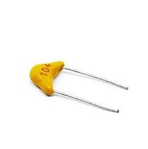
0.1/100nF – TH-Multilayer Ceramic Capacitor (Pack of 50)
The classic 100nF decoupling cap. One per IC power pin is the golden rule. This pack of 50 keeps your prototyping stock well supplied.
Placement Rules: The Golden Principles
Here are the non-negotiable rules that every PCB designer follows for decoupling capacitors:
Rule 1: Place as Close as Physically Possible
The decoupling capacitor must be placed as close to the IC power pin as the PCB layout allows — ideally within 1-2mm. The trace connecting the capacitor to the power pin is a parasitic inductor. Every extra millimetre of trace adds inductance and degrades the cap effectiveness. In high-speed designs, even 5mm of trace can render a decoupling cap nearly useless at 100MHz.
Rule 2: VCC First, Then Ground
Route the power trace from the power plane (or incoming VCC trace) to the capacitor pad first, then from the other capacitor pad to the IC power pin. This is the “VCC — Cap — IC” path. Do NOT route VCC directly to the IC and then branch to the cap; that defeats the purpose. The current path must pass through the capacitor.
Rule 3: Short, Fat Traces to Ground
The ground connection from the decoupling cap must also be low-inductance. Use a short, wide trace (or better: a via directly to a ground plane). A thin, long ground trace induces the same resonance problems as a long VCC trace.
Rule 4: Same Layer as the IC if Possible
Avoid placing your decoupling cap on the opposite side of the board from the IC if you can help it. Via inductance (typically 0.5-1nH per via) adds to the loop inductance. On a 2-layer board sometimes there is no choice, but keep vias as short as possible.
Rule 5: Do Not Share Vias Between Multiple Caps
Every decoupling cap should have its own dedicated via to the power and ground planes. Sharing a single via between two caps creates a common-mode inductance that degrades both caps simultaneously.

0.1uF Ceramic Capacitor (Pack of 50)
High-quality ceramic 0.1uF capacitors in a convenient 50-piece pack. Essential for decoupling every digital IC in your design.
Via Placement and Power Planes
On multi-layer boards with dedicated power and ground planes, via placement becomes the dominant factor in decoupling effectiveness.
Via Stitching for Ground
Place a ground via immediately adjacent to the capacitor ground pad — ideally directly under or beside the pad with a short trace of under 0.5mm. Some advanced designs use a “via in pad” technique where the via is drilled directly through the pad, minimising inductance to near zero. This requires via fill (plugging) to prevent solder wicking.
Power Plane Cutouts
If you have a power plane, route the VCC connection to the cap from the plane using a short trace stub, then continue from cap to IC. Avoid long power plane cutouts or antipads that isolate the IC from the plane — this breaks the return current path and can worsen EMI.
Two-Layer Board Strategy
On a 2-layer board without dedicated planes, dedicate wide pours on both layers to GND and VCC. Route GND on the bottom layer as a near-solid pour. This significantly reduces power distribution inductance and improves decoupling effectiveness compared to simple traces.
Multi-Capacitor Decoupling Strategy
Professional PCB designs use multiple capacitors per power pin in parallel to achieve low impedance across a wide frequency range. Here is the recommended approach:
Basic (Hobbyist/Arduino-class)
One 100nF ceramic per IC power pin. This handles most 8-16MHz microcontroller designs adequately.
Intermediate (32-bit MCUs, ESP32, STM32)
100nF ceramic + 1uF ceramic per power pin. The 1uF handles lower-frequency bulk requirements while the 100nF handles high-frequency transients. Place both close to the pin; the smaller cap (100nF) goes closer.
Advanced (High-Speed, FPGA, RF)
10nF + 100nF + 10uF per power domain. Additionally, a 100uF or larger bulk electrolytic at the power entry point to the board. Use impedance simulation tools to check the power delivery network (PDN) frequency response if your design is safety-critical.
Anti-Resonance Warning
When two capacitors of different values are placed in parallel, they can exhibit anti-resonance: a high-impedance peak at the frequency where their individual impedance curves cross. This can create a resonance spike worse than using a single cap. The fix is to choose capacitor values far enough apart in value (more than 10x ratio) and close in physical placement to minimise the loop inductance difference between them.
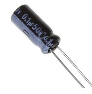
0.1uF 50V Capacitor (Pack of 50)
50V rated 0.1uF capacitors for higher-voltage supply decoupling. Pack of 50 for comprehensive PCB stock. Great for 12V and 24V logic supply filtering.
Common Mistakes and How to Avoid Them
Mistake 1: Placing Caps at the Edge of the Board
Designers sometimes place decoupling caps at the board edge or away from the IC “because there is room there.” This completely defeats the purpose. The cap must be next to the IC it is decoupling, period.
Mistake 2: Routing VCC Through the IC First
The correct current path is: Power supply — Decoupling cap — IC power pin. If you route the VCC trace to the IC and then branch to the cap (IC first, then cap), the inductance of the trace between supply and IC is not bypassed by the cap. The cap sees a direct path to ground but cannot rapidly supply the IC because it must pull current through that trace inductance first.
Mistake 3: Using Electrolytic Caps Only
Electrolytic capacitors have high ESL (equivalent series inductance) and are unsuitable for high-frequency decoupling. Their self-resonant frequency is typically in the low kHz range. Always use ceramic caps (X5R or X7R dielectric) for high-frequency bypass. Electrolytics serve a role as bulk capacitors but not as the primary HF decoupling element.
Mistake 4: Too Many Caps on Shared Vias
Daisy-chaining caps on shared power vias creates an inductive string. Each cap must have its own low-inductance path to the ground and power planes.
Mistake 5: Ignoring VCC Voltage Coefficient of Ceramics
X5R and X7R ceramics lose effective capacitance when biased at their rated voltage (DC bias effect). A 100nF X5R cap rated 10V may only provide 40-50nF of effective capacitance when used on a 5V supply. Use caps rated at least 2x the supply voltage, or use NP0/C0G ceramics for critical decoupling (though these are only available in small values).
Practical Examples: MCU and IC Decoupling
Arduino Uno / ATmega328P Style Layout
The ATmega328P has VCC (pin 7), AVCC (pin 20), and GND (pins 8, 22). Best practice:
- 100nF ceramic between VCC (pin 7) and GND (pin 8) — as close as possible
- 100nF ceramic between AVCC (pin 20) and GND (pin 22) — for the ADC supply, close to pin
- 10uF bulk near the power regulator output
ESP32 Module Decoupling
The ESP32 has multiple VDD pins and draws heavy current bursts during WiFi/BT TX. The datasheet recommends 10uF + 100nF on each VDD pin pair. Place 100nF caps on all four corners of the module footprint, with a 10uF nearby.
74HC Logic Series
Standard practice: one 100nF ceramic per 74HC IC, placed within 2mm of pin 14 (VCC) with a short trace to pin 7 (GND). For bus driver ICs like 74HC245 that drive many lines simultaneously, consider adding a second 100nF or a 10nF to handle the higher-frequency switching content.
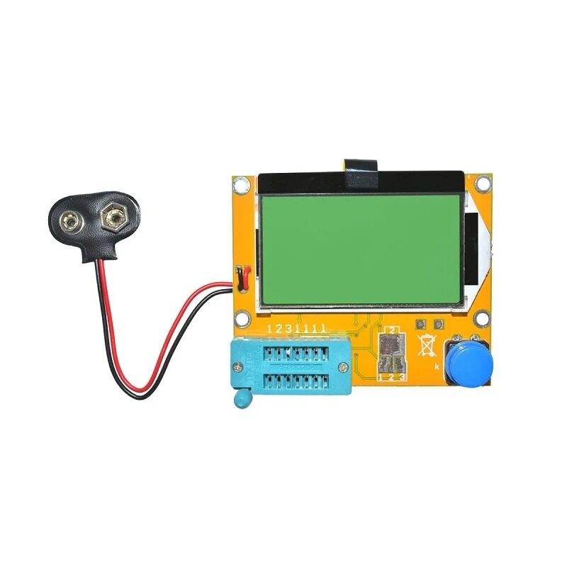
LCR-T4 12864 LCD Transistor Tester – Resistance Capacitance ESR SCR Meter
Measures actual capacitance and ESR values of your decoupling caps. Confirms caps are within spec before installing them in your PCB design.
Frequently Asked Questions
Q: Do I really need a decoupling cap for every single IC power pin?
Yes, for digital ICs switching at any meaningful frequency. The only exceptions are simple analogue circuits at very low frequencies (audio, DC amplifiers) where supply noise is less of a concern. For anything with a microcontroller, FPGA, or fast logic, one cap per power pin is the rule.
Q: Can I use a 10uF electrolytic instead of a 100nF ceramic?
No — these serve different purposes. A 10uF electrolytic has high inductance and is useless for high-frequency decoupling. It is a bulk energy reservoir, not a bypass cap. Use 100nF ceramic for high-frequency bypass and the electrolytic separately for bulk supply stabilisation.
Q: What dielectric should my decoupling caps be?
X7R or X5R for values 100nF to 10uF. These have good capacitance stability over temperature. Avoid Y5V and Z5U — they have terrible DC bias and temperature coefficients that can reduce effective capacitance by 80% at operating conditions. For sub-10nF values, NP0/C0G is preferred for its stability.
Q: My schematic shows a single power net — do I need decoupling on every IC that connects to it?
Yes. The schematic is a logical representation; the physical PCB has resistance and inductance in every trace. Even though every IC shares the same schematic net, each one needs its own local decoupling cap to handle its own switching transients without disturbing its neighbours.
Q: How do I verify my decoupling is working?
Use an oscilloscope with a 10:1 probe, measure the power supply pin of your IC under load conditions. You should see very small ripple (under 100mV for most digital logic). If you see large spikes correlated with switching activity, your decoupling is insufficient or misplaced.
Stock up on decoupling essentials from Zbotic.in. We carry ceramic capacitors in all popular values — 100nF, 10nF, 1uF, and 10uF — in packs suitable for both prototyping and small production runs. Shop capacitors and passive components with fast delivery across India.


Add comment