
Gate Driver IC: Isolated and Non-Isolated MOSFET Drive
A gate driver IC for MOSFET switching is one of those unsung heroes of power electronics — often overlooked by beginners but critically important for making high-speed switching work reliably. Whether you’re building a motor driver, DC-DC converter, inverter, or class-D audio amplifier, the gate driver IC is what stands between your microcontroller’s 3.3V logic signal and the MOSFET’s power gate. Get it wrong and you’ll face slow switching, shoot-through current, overheating, and failed MOSFETs. Get it right, and your circuit switches cleanly, efficiently, and reliably. This guide covers everything Indian makers and engineers need to know about both isolated and non-isolated gate driver ICs.
Why Do MOSFETs Need a Gate Driver?
A MOSFET’s gate is capacitive — the gate-to-source capacitance (Cgs) and gate-to-drain capacitance (Cgd, the Miller capacitance) must be charged and discharged rapidly for fast switching. The total gate charge (Qg) that must be moved each switching cycle determines the switching speed.
For a typical power MOSFET like the IRFZ44N:
- Total gate charge Qg = 63 nC
- Threshold voltage Vgs(th) ≈ 4V; full enhancement at Vgs = 10V
- At 100 kHz switching, gate charge current needed: Ig = Qg × f = 63 nC × 100,000 = 6.3 mA average
- But peak current during the Miller plateau can spike to 0.5–2A for fast transitions
A microcontroller GPIO pin (Arduino, STM32) can only source/sink 8–20 mA. This severely limits switching speed, causing:
- Slow rise/fall times at the gate → extended switching transitions → massive switching losses
- Excessive heat in the MOSFET during transitions
- Unreliable turn-on at high switching frequencies (the MOSFET may not fully enhance)
- Miller capacitance coupling noise back into the control signal
A dedicated gate driver IC solves all of these problems by providing peak current capability of 1A to 10A directly at the MOSFET gate, making transitions in 10–50 ns instead of microseconds.
Non-Isolated Gate Drivers: Types and Operation
Non-isolated gate drivers share a common ground reference between the control signal and the gate output. They are the simplest and most commonly used type for low-side switch driving and bootstrap-based half-bridge configurations.
Low-Side Single-Channel Drivers
These drive a single MOSFET whose source is connected to ground. The control logic input references the same ground as the driver output. Examples: TC4420, UCC27524, TC427. Typical peak output current: 1.5–4A. Used in flyback converters, buck converters, and inductive load drivers.
Dual-Channel Drivers (IN+ and IN-)
A single package containing two gate drivers — useful for totem-pole configurations or when driving two independent MOSFETs. Examples: UCC27524 (dual, same input), TC4427 (dual, inverting and non-inverting).
Half-Bridge Drivers
Drive both the high-side and low-side MOSFET of a half-bridge (two MOSFETs in series, drain of high-side to rail, source of low-side to ground, switching node in between). The high-side driver typically uses a bootstrap circuit (see next section). Examples: IR2101, IR2110, IRS2183S, L6387. These are the workhorses of motor drives and DC-DC converter designs.
Full-Bridge / H-Bridge Drivers
Drive all four MOSFETs of an H-bridge for bidirectional motor control or single-phase inverter output. Examples: IR2136, DRV8300. Often include dead-time insertion to prevent shoot-through.
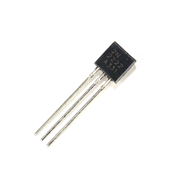
2N2222 NPN Transistor (Pack of 20)
For low-speed MOSFET gate drive on small signal applications, a simple NPN transistor stage (totem-pole with PNP) can serve as a budget gate driver. Pack of 20 for prototyping.
Bootstrap Gate Drivers: Driving High-Side MOSFETs
The high-side MOSFET in a half-bridge presents a unique challenge: its source terminal (the switching node) swings between ground and the supply rail. The gate must be driven at Vgs above this floating source — which means the gate drive voltage must “float” up and down with the switch node.
The bootstrap technique solves this elegantly:
How Bootstrap Circuits Work
- A small bootstrap capacitor (Cboot, typically 100nF–470nF) is connected between the switch node (VS pin) and the high-side gate driver supply (VB pin).
- When the low-side MOSFET turns on, the switch node is pulled to ground. A diode (bootstrap diode) from the 15V rail through the capacitor charges Cboot to approximately 15V.
- When the high-side MOSFET turns on and the switch node rises, Cboot floats up with it — its voltage (referenced to the switch node) remains at ~15V, providing the gate drive voltage above the switch node level.
- Each time the low-side turns on, Cboot recharges, replenishing any charge lost through the gate drive of the high-side MOSFET.
Bootstrap Diode Selection
The bootstrap diode must be a fast-recovery or Schottky type to minimise charge loss and prevent reverse conduction during high-side switching. Avoid standard 1N4007 — its slow recovery injects charge and reduces bootstrap effectiveness. Use 1N4148, US1M, or the integrated bootstrap diode in devices like the IR2110.
Bootstrap Limitations
- 100% duty cycle is impossible — the low-side must turn on periodically to recharge Cboot. In duty-cycle limited applications, charge pump circuits replace the bootstrap.
- Voltage rating: Cboot must be rated above the maximum switch node voltage swing (full rail voltage). Use 50V or 100V-rated ceramic capacitors even in a 12V system for surge protection.
- Under-voltage lockout (UVLO): If Cboot discharges too much, UVLO in the driver IC inhibits gate drive — add a charge pump or reduce dead time if this occurs.
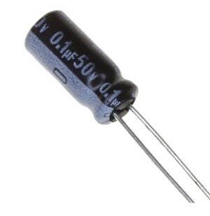
0.1µF 50V Capacitor (Pack of 50)
Perfect voltage rating for bootstrap capacitors in 12V–48V motor drivers and half-bridge converters. Also ideal for gate driver supply decoupling.
Isolated Gate Drivers: When and Why
Isolated gate drivers include a galvanic isolation barrier between the input control signal and the gate drive output. This isolation is implemented using one of three technologies:
1. Optocoupler-Based Isolation
Traditional isolation using an LED-photodetector pair. The HCPL-3120 (Broadcom) and ACNW3190 are classic high-current optocoupler gate drivers. Advantages: lowest cost, very high isolation voltage (5000V). Disadvantages: slow propagation delay (typically 1–3 µs), temperature drift of LED current, limited common-mode transient immunity (CMTI).
2. Transformer-Based Isolation
A tiny ferrite pulse transformer provides isolation with very low propagation delay (~100 ns). Examples: ADuM1234 series (Analog Devices uses iCoupler magnetic coupling), Si8230 (Silicon Labs). Excellent CMTI, fast, but requires a separate isolated power supply for the output stage, or an integrated DC-DC converter inside the package.
3. Capacitive Isolation
Uses on-chip high-voltage capacitors for signal coupling. TI’s ISO7xxx series, Analog Devices’ ADuM series. Extremely fast (sub-100 ns), high CMTI, small package. Power must still be provided to the isolated side.
When Do You Need Isolated Gate Drivers?
Use isolated gate drivers when:
- High-side of a mid-point or H-bridge switches above 100V — bootstrap becomes inadequate for wide duty-cycle ranges or high rail voltages
- Safety isolation is required — mains-connected motor drives, grid-tied inverters, medical equipment
- Three-phase inverters — each of the six switches (in a 3-phase bridge) needs individually isolated gate drive
- SiC/GaN MOSFETs — wide-bandgap devices switch so fast (dv/dt > 50V/ns) that CMTI becomes critical; only the best isolated drivers (CMTI > 100V/ns) work reliably
- Long cable runs between controller and power stage — isolation breaks ground loop noise coupling
How to Select a Gate Driver IC
Use this checklist to select the right gate driver for your application:
1. Output Peak Current
Calculate required gate current for your target rise time:
Ig_peak = Qg / tr
For IRFZ44N (Qg = 63 nC) with 50 ns rise time: Ig_peak = 63 nC / 50 ns = 1.26A
Choose a driver rated at least 1.5–2× this: a 2A or 3A driver provides margin.
2. Propagation Delay and Matching
In half-bridge configurations, mismatched propagation delays between high-side and low-side drivers cause asymmetric dead time, which can lead to shoot-through or duty cycle errors. Choose drivers with specified and matched propagation delays, or use a dedicated half-bridge driver IC that inherently matches both channels.
3. Input Logic Compatibility
Most modern gate drivers accept CMOS/TTL input levels (3.3V or 5V compatible). Verify the input threshold (VIH, VIL) matches your microcontroller’s output levels. Some drivers require 5V logic while your MCU outputs 3.3V — use a driver with 3.3V-compatible inputs or add a level shifter.
4. Supply Voltage
Standard silicon MOSFETs need Vgs = 10–15V for full enhancement. SiC MOSFETs may need +15V/-5V (split supply). GaN HEMTs need only 5–7V. Match the gate driver’s output supply to your MOSFET’s requirements.
5. Dead Time Control
Drivers for half-bridge applications must include programmable dead time to prevent both MOSFETs from conducting simultaneously (shoot-through). Look for drivers with external resistor or capacitor dead time programming, or fixed dead-time insertion.
6. Protection Features
Premium gate driver ICs include: Under-Voltage Lockout (UVLO), Short-Circuit / Desaturation Protection (for IGBTs), Active Miller Clamp (prevents spurious turn-on due to Miller capacitance), and Fault reporting output.
Popular Gate Driver ICs in India
| IC | Type | Peak Current | Key Feature |
|---|---|---|---|
| IR2101 | Half-bridge, bootstrap | 130mA/270mA | Budget, DIP-8, widely available |
| IR2110 | Half-bridge, bootstrap | 2A/2A | Classic choice, separate LO/HO enables |
| TC4420/TC4422 | Single, low-side | 6A | High current, TO-220 and SOIC |
| UCC27524 | Dual, low-side | 5A | Fast 13ns rise time, TTL and CMOS input |
| HCPL-3120 | Isolated, optocoupler | 2A | 5000V isolation, IGBT/MOSFET compatible |
| ADuM3223 | Isolated, magnetic | 4A | 5kV isolation, 100kV/µs CMTI |
| Si8234 | Isolated, half-bridge | 4A | Integrated DC-DC for isolated Vcc |
| IRS2183S | Half-bridge, bootstrap | 1.7A/1.7A | Small SOIC-8, 600V operation |
PCB Layout Considerations
Gate driver PCB layout is as important as the IC selection. Poor layout introduces gate oscillations, common-mode noise, and reliability problems.
Gate Resistor (Rg)
Add a series gate resistor (5–33 Ω) between the driver output and the MOSFET gate. This:
- Limits peak gate current to prevent driver latch-up
- Damps gate-source ringing (gate lead inductance + Cgs forms an LC resonator)
- Controls dv/dt at the switching node (useful for EMI reduction and preventing Miller-induced turn-on of the complementary switch)
Use separate gate-on (Rg_on) and gate-off (Rg_off) resistors via a diode if asymmetric turn-on/turn-off is desired — faster turn-off reduces cross-conduction risk.
Gate Driver Supply Decoupling
Place a 100 nF ceramic capacitor as close as possible to the Vcc-GND pins of the gate driver IC. For high-current drivers (above 2A), add a 4.7 µF bulk capacitor in parallel. The gate driver’s supply current has high-frequency pulses — decoupling capacitors must be on the same PCB layer with minimal trace inductance.
Kelvin Source Connection
Connect the gate driver ground return (reference) directly to the MOSFET source pin with a dedicated trace — this is called Kelvin connection. Do not share this trace with the power current path. The source inductance in the power path creates a voltage drop (Lsource × di/dt) that appears as negative Vgs feedback, slowing turn-on. A Kelvin source connection eliminates this effect.
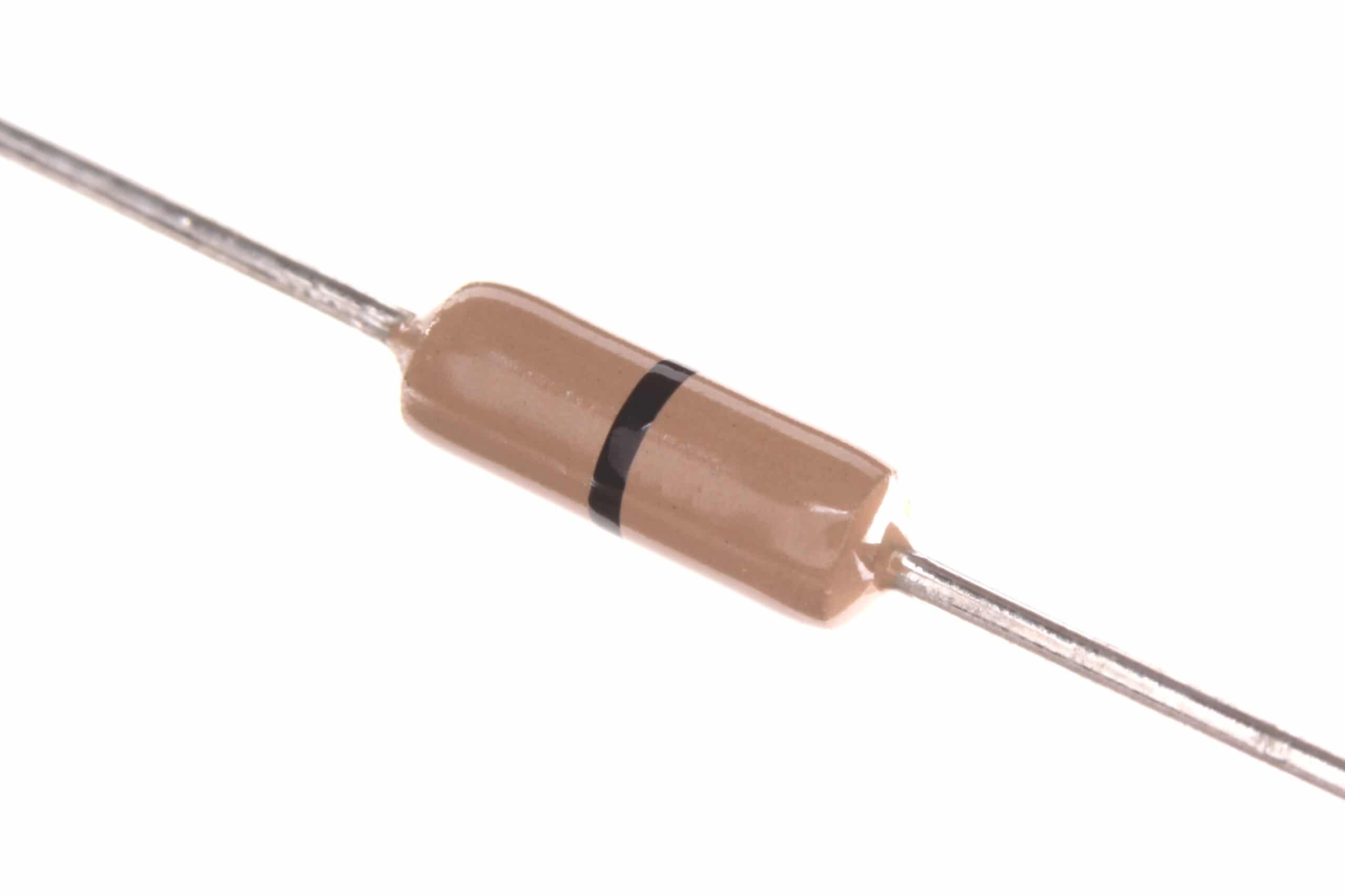
0 Ohm 0.25W Carbon Film Resistor (Pack of 100)
Use as solder-in jumpers for gate resistor positions during prototyping, or to test zero-resistance baseline switching performance before adding gate resistors.
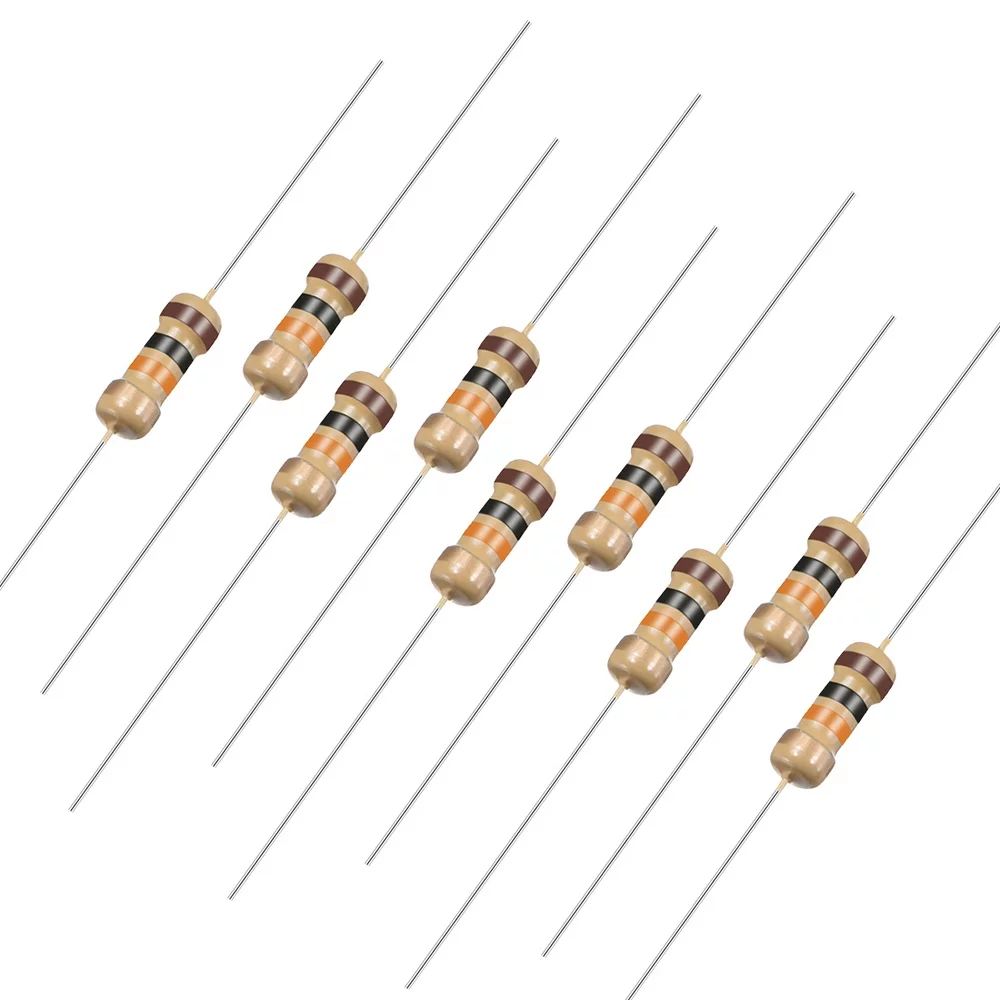
10 Ohm 0.25W Carbon Film Resistor (Pack of 50)
10 Ohm is a commonly used value for gate series resistors in low to medium power MOSFET drivers. Good starting point for slew rate control during prototyping.
Frequently Asked Questions
Q1: Can I drive a MOSFET directly from an Arduino GPIO pin?
For very low switching frequencies (below 1 kHz) and small signal MOSFETs (like the 2N7000 or BS170 with very low gate charge of 1–2 nC), an Arduino GPIO can provide adequate drive. For power MOSFETs in switching converters or motor drives (where fast switching matters), you must use a dedicated gate driver IC. The Arduino GPIO’s ~20 mA current limit produces unacceptably slow transitions in power MOSFETs, causing excessive heat and potential MOSFET failure.
Q2: What is shoot-through in an H-bridge and how does a gate driver prevent it?
Shoot-through (also called cross-conduction) occurs when both the high-side and low-side MOSFETs in a half-bridge leg conduct simultaneously, creating a short circuit from supply to ground. This instantly destroys MOSFETs. Gate driver ICs prevent it by inserting “dead time” — a brief period where both switches are off during the transition. Quality half-bridge drivers (like IR2110, IRS2183) include hardware dead time generation that cannot be bypassed by software bugs, providing reliable protection.
Q3: What is Common-Mode Transient Immunity (CMTI) in isolated gate drivers?
CMTI specifies the maximum rate of change of voltage (dv/dt) across the isolation barrier that the driver can tolerate without false triggering. Measured in V/µs or kV/µs. In a high-speed half-bridge, the switch node slams from 0V to the full rail voltage in nanoseconds — this dv/dt couples through stray capacitance across the isolation barrier. If the CMTI is too low, the driver falsely triggers the MOSFET. SiC-based power stages need isolated drivers with CMTI > 100 kV/µs (e.g., ADuM3223, Si827x series).
Q4: How do I choose between a bootstrap-based gate driver and a fully isolated driver?
Use bootstrap (e.g., IR2110) when: supply voltage is under 600V, duty cycle is not near 100% (so Cboot can recharge), and cost minimisation is critical. Use fully isolated drivers when: duty cycle approaches 100%, supply voltage is above 600V (e.g., SiC inverters at 800V), safety isolation is required, or common-mode noise immunity must be guaranteed regardless of duty cycle. Isolated drivers cost more (₹150–₹500 per channel vs ₹20–₹50 for bootstrap) but provide unconditional reliability.
Q5: What is the Miller effect and why does it matter for gate driver design?
The Miller effect refers to the amplification of the gate-drain capacitance (Cgd) due to the drain voltage swing. During switching, as Vds changes rapidly, a current i = Cgd × dVds/dt flows through Cgd into the gate node. If the gate driver can’t sink this current quickly enough, the gate voltage bounces up — possibly turning on the complementary switch (spurious turn-on). Solutions: use a strong gate driver with high sink current, add a negative gate drive voltage (e.g., -5V turn-off for SiC MOSFETs), or use an Active Miller Clamp circuit that holds the gate of the off-state MOSFET firmly at turn-off voltage.
Build Your Motor Drive or Power Converter with Zbotic
Zbotic stocks resistors, capacitors, transistors, and all the passive components needed to complete your gate driver circuit. Start your motor controller or SMPS project with quality components delivered fast across India.


Add comment