
Every year, electrostatic discharge (ESD) silently destroys millions of rupees worth of electronic components globally — and a significant portion of those losses happen in home workshops, college labs, and small-scale manufacturing setups across India. Understanding ESD protection in electronics is not optional if you want your ICs, MOSFETs, microcontrollers, and precision sensors to survive from the workbench to the final product.
The frustrating part is that ESD damage is often invisible. A component zapped by static may still appear to function initially, but it develops latent failures that cause erratic behaviour or premature death days or weeks later — leading to hours of wasted debugging. This guide covers exactly what ESD is, how it destroys components, and the practical steps every maker and engineer in India should take to prevent it.
Table of Contents
- What Is ESD and How Does It Damage ICs?
- Which Components Are Most Vulnerable?
- Common ESD Sources in the Indian Workshop
- Personal Grounding: Wrist Straps and Heel Straps
- Setting Up an ESD-Safe Workspace
- Safe Component Handling Techniques
- On-Circuit ESD Protection Techniques
- Storage and Packaging for ESD-Sensitive Parts
- Frequently Asked Questions
What Is ESD and How Does It Damage ICs?
Electrostatic discharge (ESD) is the sudden flow of electricity between two objects at different electrostatic potentials — essentially a miniature lightning strike. When you walk across a carpet in rubber-soled shoes and then touch a door handle, you feel a tiny shock: that is ESD. Your body can build up voltages of 2,000V to 35,000V depending on humidity, materials, and movement — all invisible and unfelt until discharge occurs.
Modern ICs operate at 1.8V to 5V with gate oxides just a few nanometres thick. A discharge of even 100V through a MOSFET gate oxide can punch a microscopic hole through it, permanently destroying the transistor. The energy involved is tiny (millijoules) — you will not feel it, but the IC cannot survive it.
ESD failure modes include:
- Catastrophic failure — immediate, visible damage. The component fails immediately and obviously (dead on arrival).
- Latent failure — partial damage. The component appears to work but has reduced noise margins, increased leakage, or weakened junctions that fail under stress weeks later. This is the most dangerous failure mode because it is nearly impossible to diagnose without specialised equipment.
- Upset — temporary malfunction without permanent damage. The circuit resets or behaves erratically during an ESD event, then recovers. This is the mildest form but still indicates your protection is inadequate.
Which Components Are Most Vulnerable?
Not all components are equally sensitive to ESD. Roughly, ESD sensitivity is classified by the Human Body Model (HBM) voltage threshold — the voltage at which damage occurs:
| Sensitivity Class | HBM Threshold | Typical Components |
|---|---|---|
| Class 0 (Extremely sensitive) | <250V | GaAs FETs, microwave transistors, some MEMS sensors |
| Class 1 (Very sensitive) | 250V – 500V | MOSFET ICs, CMOS logic, precision op-amps |
| Class 2 (Sensitive) | 500V – 2000V | ESP32, STM32, nRF modules, most microcontrollers |
| Class 3 (Less sensitive) | 2000V – 4000V | BiCMOS and some bipolar ICs |
| Not sensitive | >4000V | Resistors, inductors, ceramic capacitors (mostly) |
Note that passive components like resistors, ceramic capacitors, and standard inductors are generally not ESD-sensitive. However, electrolytic capacitors can be damaged by reverse polarity or voltage spikes associated with ESD events.
Common ESD Sources in the Indian Workshop
Indian workshops and home labs often have conditions that are worse for ESD than professional electronics manufacturing environments:
- Low humidity. In air-conditioned rooms during Indian summers (AC dries the air), relative humidity can fall to 30–40%. ESD generation increases dramatically below 50% RH.
- Synthetic flooring and clothing. Polyester and nylon carpets and clothing are strong charge generators. The traditional plastic chair with rubber feet used at most workbenches is an effective charge accumulator.
- Plastic component storage boxes. Standard plastic boxes, trays, and even component tape/reels are insulating and can charge up ICs placed inside them.
- Working without a wrist strap. The most common and most impactful omission. Without a wrist strap, the human body is the primary ESD source.
- Soldering iron tips. An ungrounded or poorly grounded soldering iron can deliver thousands of volts through its tip to a component being soldered.
Personal Grounding: Wrist Straps and Heel Straps
The single most effective ESD prevention measure is personal grounding. A wrist strap consists of a conductive band worn on your wrist connected to ground via a coiled cable and a 1MΩ series resistor. The resistor limits current to safe levels while still draining static charge.
Key points about wrist straps:
- Always connect to earth ground, not to circuit ground. Use the earth pin of a properly earthed Indian power outlet (the round bottom pin in a 15A socket or the large top pin in older sockets).
- Check the strap regularly. The conductive band degrades with sweat and wear. Most wrist straps include a tester that confirms continuity. Test before each use.
- Wear it on bare skin. Wearing over a thick shirt sleeve reduces its effectiveness significantly. It must contact your skin for proper static drainage.
- Heel straps and ESD footwear are used when you need to move around during work. They work with ESD-safe flooring to maintain grounding while standing or walking.
Setting Up an ESD-Safe Workspace
A proper ESD-safe workspace (EPA — ESD Protected Area) includes several layers of protection:
ESD Mat
An ESD-dissipative rubber mat on your workbench provides a grounded work surface. Components placed on this mat are quickly drained of static charge. The mat connects to ground via a coiled cable (usually with a common ground point shared by your wrist strap). ESD mats come in various sizes; a 60×90cm mat covers most hobby workbenches.
Grounded Soldering Iron
Ensure your soldering iron’s tip is at ground potential. Better quality soldering stations include a grounding connection for the tip. A poorly grounded or floating tip is a significant ESD risk, especially when soldering CMOS ICs or SMD components directly on a PCB.
Ioniser (Optional but Effective)
An ESD ioniser blows a stream of ionised air over the work area, neutralising charges that cannot be drained by grounding (such as on insulating objects). Ionisers are standard equipment in professional electronics manufacturing but are less common in hobby setups. For high-value or extremely sensitive components, an ioniser is worth the investment.
Humidity Control
Maintaining relative humidity above 45–50% significantly reduces ESD generation. A basic room humidifier can make a measurable difference in dry Indian winter or air-conditioned environments. This is a low-cost, high-impact improvement for labs where ESD mats and wrist straps are already in use.
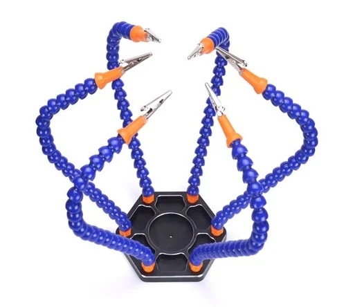
6 Flexible Arms Soldering Station With Swiveling Alligator Clip
A proper helping-hands soldering station keeps components securely positioned during soldering, reducing accidental contact with ungrounded surfaces — an important part of ESD-safe soldering practice.
Safe Component Handling Techniques
Even with a wrist strap and mat, handling technique matters:
- Handle ICs by the body, not the pins. The leads are the entry points for ESD — minimise contact with them.
- Keep components in their original ESD-safe packaging until the moment you need them. Anti-static bags, conductive foam, and tape-and-reel packaging are all designed to prevent charge buildup.
- Do not slide ICs across insulating surfaces. Sliding a MOSFET across a plastic table can charge it to thousands of volts in an instant.
- Touch grounded metal before handling sensitive parts. If you do not have a wrist strap, at least touch the chassis of your power supply or a grounded metal surface before picking up an IC. This drains your body charge temporarily.
- Insert ICs last when building on a breadboard. Complete all wiring with power off, then insert the IC. This minimises the time the IC pins are exposed and reduces ESD risk from incidental contact during wiring.
On-Circuit ESD Protection Techniques
Beyond workbench precautions, you should also design ESD protection into circuits that interface with the outside world — connectors, buttons, sensors, and any pin accessible to a user.
TVS (Transient Voltage Suppressor) Diodes
TVS diodes clamp voltage spikes to a safe level. For a 3.3V signal line, use a unidirectional TVS rated at 3.3V standoff voltage — it clamps anything above ~3.6–3.8V to ground. Place the TVS as close to the connector or external-facing pin as possible.
Series Resistors on I/O Lines
A 22–100Ω resistor in series with each I/O pin connected to the outside world limits the peak current of an ESD event reaching the IC. Simple, cheap, and effective as a first line of defence.
ESD Protection ICs
Dedicated ESD protection ICs (such as the PRTR5V0U2X or TPD4E004) contain arrays of clamping diodes optimised for specific interfaces (USB, HDMI, I2C, SPI). They are the correct choice for high-speed interfaces where series resistors would cause signal integrity problems.
Ground Plane
A continuous ground plane on a PCB provides a low-impedance discharge path that limits the extent of ESD damage. It also acts as a shield against RF-induced interference. If you are designing your own PCB in KiCad or EasyEDA, always include a ground plane.
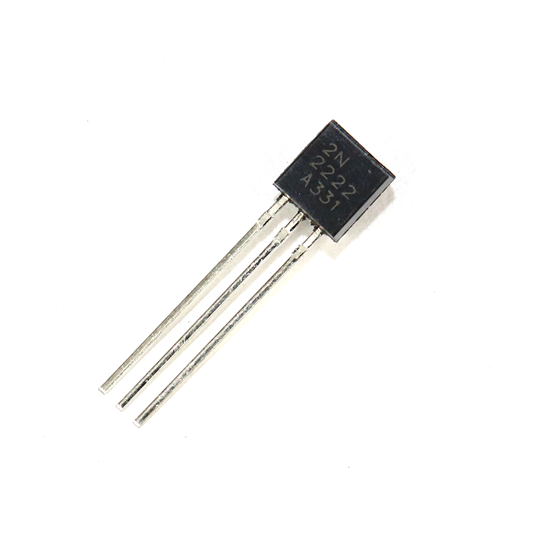
2N2222 NPN Transistor (Pack of 20)
The 2N2222 has good ESD robustness for a general-purpose transistor. Understanding ESD ratings helps you choose the right transistor for exposed I/O interfaces in your designs.
Storage and Packaging for ESD-Sensitive Parts
Components are at risk not just during handling but during storage. Follow these guidelines:
- Anti-static bags (pink polyethylene): The standard black/silver metallic bags are best (conductive shielding). Pink anti-static bags are dissipative but not shielding — use them only when not exposed to strong external fields.
- Conductive foam: Excellent for ICs with through-hole pins (DIP packages). The foam conducts charge away from the pins gently. Never use standard household foam — it is highly insulating and can charge components up to thousands of volts.
- Labelled ESD boxes: If you bulk-store SMD components, use ESD-rated component boxes with dissipative materials. Avoid standard hard plastic storage boxes for ICs and MOSFETs.
- Temperature and humidity: Store ICs in a cool, dry, but not air-conditioned environment. Extreme dryness increases ESD risk; extreme humidity risks moisture-induced failures when the component is later soldered (moisture-sensitivity levels, or MSL, are a related topic).
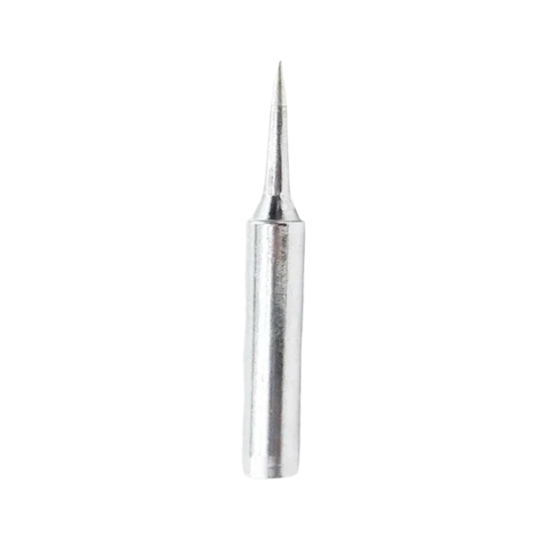
BAKON Soldering Iron Tip 900M-T-I
A quality soldering iron tip that maintains consistent tip temperature and grounding — both critical for ESD-safe soldering of CMOS ICs and sensitive SMD components.
Frequently Asked Questions
Can ESD damage an Arduino or Raspberry Pi?
Yes, though these boards include some on-chip ESD protection. The microcontrollers and SoCs on these boards are CMOS devices. GPIO pins directly connected to the outside world (via jumper wires or connectors) are the most vulnerable points. Touching a GPIO pin without a wrist strap while your body carries static charge can cause latent damage that shows up as erratic I/O behaviour or sensor reading errors later.
How do I know if a component was damaged by ESD?
Catastrophic ESD damage is obvious — the component simply does not work. Latent damage is much harder to detect. Signs include: intermittent or erratic behaviour, higher-than-specified power consumption, reduced operating frequency, unexpected resets under specific conditions, or abnormal pin-to-pin leakage resistance (measurable with a high-quality multimeter on the resistance setting).
Is an anti-static wrist strap necessary at home, or just in factories?
For resistors, capacitors, and through-hole LEDs — not really necessary. For MOSFETs, CMOS ICs, ESP32/ESP8266 modules, STM32 microcontrollers, RF modules, and any component with gates thinner than 50nm — a wrist strap is strongly recommended even at home. The cost is under ₹200 and can save components worth hundreds or thousands of rupees.
Does touching a grounded surface before handling components provide enough protection?
It helps, but it is temporary. Static charge rebuilds on your body within seconds of movement. A wrist strap provides continuous drainage, which is what truly protects components throughout the handling process.
Are ESD bags reusable?
Standard metallic ESD bags degrade after many uses and punctures. If a bag is visibly damaged, cut, or punctured, discard it. For long-term storage, use hard ESD-rated containers. The shielding effectiveness of a damaged bag is compromised even if it looks usable.
Protect Your Components, Protect Your Projects
ESD protection is one of those foundational practices that separates experienced makers from frustrated beginners. Implementing even the basic measures — a wrist strap, an ESD mat, and careful handling — eliminates the majority of static-related component losses and the hours of debugging that follow them.
Zbotic stocks a full range of electronic components suitable for ESD-sensitive projects, all packaged properly for safe delivery across India. Explore our Electronics Basics category for resistors, capacitors, transistors, and tools to build your ESD-safe workspace from scratch.


Add comment