
BJT Biasing Methods: Fixed, Voltage Divider and Emitter Bias
The Bipolar Junction Transistor (BJT) is the workhorse of analogue electronics, but it only performs correctly when it is properly biased. Understanding BJT biasing methods is fundamental for anyone designing amplifiers, oscillators, or switching circuits. Without stable DC operating conditions — the Q-point — your transistor will distort signals, clip waveforms, or simply refuse to work. In this comprehensive guide, we cover every major BJT biasing technique: fixed bias, collector-to-base bias, voltage divider bias, and emitter bias. We’ll analyse each method with equations, explain stability factors, and show you how to choose the right approach for your project.
What Is BJT Biasing and Why Does It Matter?
A BJT has three operating regions: cut-off (fully off), saturation (fully on), and active (linear amplification zone). For analogue applications like audio amplifiers, the transistor must operate in the active region with the correct DC voltages and currents established before any AC signal is applied. These DC conditions define the quiescent point or Q-point (V_CE, I_C).
The challenge is that BJT parameters — especially the current gain β (hFE) — vary enormously between individual transistors of the same part number (e.g., BC547 has β ranging from 110 to 800), and they shift with temperature. A biasing circuit must hold the Q-point stable despite these variations. This is measured by the stability factor S = ΔI_C / ΔI_CO, where lower S indicates better stability.

BC547 NPN 100mA Transistor TO-92 (Pack of 10)
The BC547 is the most popular NPN transistor in India for biasing experiments and amplifier projects. With β ranging 110–800, it’s ideal for learning how different bias networks handle β variability.
Fixed Bias (Base Bias)
Fixed bias is the simplest BJT biasing method, using a single resistor (RB) connected between the supply voltage VCC and the base of the transistor.
Circuit and Equations
The base current is set by:
I_B = (V_CC − V_BE) / R_B
I_C = β × I_B
V_CE = V_CC − I_C × R_C
Choosing a Q-point at V_CE = V_CC/2 (midpoint for maximum undistorted swing) and a desired I_C, you can solve for R_B and R_C directly.
Design Example: VCC = 12V, desired I_C = 2 mA, β = 200, V_BE = 0.7V
R_C = (12 − 6) / 0.002 = 3kΩ
I_B = 2 mA / 200 = 10 µA
R_B = (12 − 0.7) / 10 µA = 1.13 MΩ (use 1 MΩ)
Advantages and Disadvantages
Advantages: Only one resistor needed; simple calculation; lowest component count.
Disadvantages: The stability factor S = 1 + β, which means if β doubles (due to transistor replacement or temperature rise), I_C also doubles. The Q-point shifts dramatically — making fixed bias unsuitable for most analogue designs. Use it only for switching circuits where exact Q-point doesn’t matter.
Collector-to-Base Bias (Feedback Bias)
In collector-to-base bias, the base resistor RB is connected to the collector instead of VCC. This provides negative feedback that partially stabilises the Q-point.
How It Works
If temperature rises and I_C tries to increase, V_CE drops (because V_CE = VCC − I_C×RC). Since V_CE appears at the top of RB, the base current I_B = (V_CE − V_BE) / RB also decreases, which reduces I_C and partially counteracts the original increase. This self-correcting mechanism is what makes it better than fixed bias.
I_B = (V_CC − V_BE) / (R_B + (1 + β) × R_C)
I_C = β × I_B
V_CE = V_CC − I_C × R_C
Stability factor S = (1 + β) / (1 + β × RC/(RB + RC)). Better than fixed bias but still β-dependent.
Best Use Cases
Collector-to-base bias is a good compromise where you need simplicity but better stability than pure fixed bias — for example, in small RF pre-amplifier stages or signal conditioning circuits where exact Q-point isn’t critical but gross Q-point drift must be avoided.
Voltage Divider Bias — The Most Stable Method
Voltage divider bias (also called potential divider bias) is by far the most widely used BJT biasing method in practical circuit design. It uses two resistors (R1 and R2) to establish a stable base voltage that is largely independent of β.
Circuit Analysis
The key insight is that when the current through R1–R2 is much larger than the base current (typically 10× or more), the Thevenin voltage at the base is approximately:
V_TH = V_CC × R2 / (R1 + R2)
R_TH = R1 ∥ R2 = (R1 × R2) / (R1 + R2)
I_C ≈ (V_TH − V_BE) / R_E
V_CE = V_CC − I_C × (R_C + R_E)
Notice that I_C depends on V_TH, V_BE, and R_E — none of which depend on β! This is why voltage divider bias achieves near-β-independent Q-point stability.
Step-by-Step Design Procedure
- Choose I_C and V_CE: Set V_CE = VCC/2 for maximum swing. If VCC = 12V, set V_CE = 6V.
- Choose V_E: V_E ≈ 0.1 × VCC (10% of supply). V_E = 1.2V for 12V supply.
- Calculate R_E: R_E = V_E / I_E ≈ V_E / I_C (since I_E ≈ I_C for high β). For I_C = 2 mA: R_E = 1.2V / 2 mA = 600Ω → use 560Ω or 620Ω.
- Calculate R_C: V_RC = V_CC − V_CE − V_E = 12 − 6 − 1.2 = 4.8V. R_C = 4.8V / 2 mA = 2.4kΩ → use 2.2kΩ.
- Calculate V_B: V_B = V_E + V_BE = 1.2 + 0.7 = 1.9V.
- Choose R1 and R2: I_divider ≥ 10 × I_B. For β = 200, I_B = 10 µA, so I_divider ≥ 100 µA. R1 + R2 = 12V / 100 µA = 120kΩ. R2 = 1.9V × 120kΩ / 12V = 19kΩ → use 18kΩ. R1 = 120 − 18 = 102kΩ → use 100kΩ.
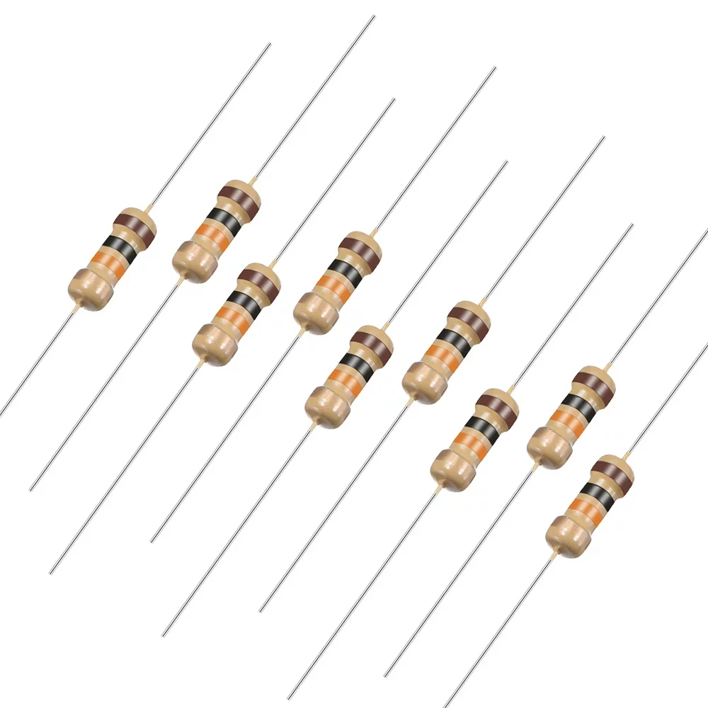
0 Ohm 0.25W Carbon Film Resistor (Pack of 100)
Zero-ohm jumpers are useful for breadboard prototyping when testing BJT bias circuits — use them as programmable wire links to swap between bias configurations without rewiring the board.
The Role of the Emitter Bypass Capacitor
R_E provides DC feedback that stabilises the Q-point, but it also reduces AC voltage gain because it introduces negative AC feedback. To restore the AC gain without losing DC stability, connect a large bypass capacitor (CE, typically 10–100 µF electrolytic) in parallel with R_E. At signal frequencies, CE acts as a short circuit, effectively removing R_E from the AC equivalent circuit while keeping it in place for DC analysis.
The AC gain with bypass cap: Av = −β × RC / r_e where r_e = 26 mV / I_C
For I_C = 2 mA: r_e = 13Ω, Av = −200 × 2200 / 13 ≈ −338 (about 50 dB)
Emitter Bias with Dual Supply
Emitter bias uses a split (dual) power supply (+VCC and −VEE) to bias the BJT. The emitter resistor RE connects to the negative supply −VEE, which provides a fixed emitter voltage without requiring R1 and R2.
Analysis
I_E = (V_EE − V_BE) / (R_E + R_B/β)
V_CE = V_CC + V_EE − I_C × (R_C + R_E)
When R_B is small and β is large, I_E ≈ V_EE / R_E, making the emitter current highly independent of β. The stability factor approaches S ≈ 1, which is the theoretical minimum — perfect Q-point stability.
Where Emitter Bias Is Used
- Op-amp input stages that require dual supply rails
- Class AB push-pull output stages in audio amplifiers
- Differential amplifier pairs — one of the most important building blocks in analogue IC design
The downside is the requirement for a dual supply, which adds complexity to bench designs but is common in op-amp circuit work.
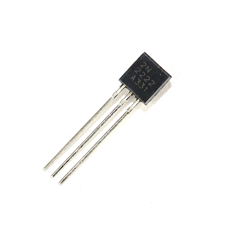
2N2222 NPN Transistor (Pack of 20)
The 2N2222 is an excellent transistor for biasing experiments due to its predictable characteristics. Use it alongside BC547 to compare how β variation between part numbers affects each bias configuration.
Stability Factor S: Comparing All Methods
The stability factor S quantifies how much the collector current I_C changes with respect to the reverse leakage current I_CO (which doubles approximately every 10°C). Lower S is better.
| Biasing Method | Stability Factor S | Practical Range | Best Application |
|---|---|---|---|
| Fixed Bias | S = 1 + β | 100–800 | Digital switching only |
| Collector-to-Base | S = (1 + β) / (1 + β×RC/(RB+RC)) | 5–50 | Simple RF pre-amps |
| Voltage Divider | S ≈ 1 + RTH/RE | 1–10 | Most analogue applications |
| Emitter Bias (Dual Supply) | S ≈ 1 | ≈1 | High-stability, dual-supply circuits |
Practical Design Example
Let’s design a complete voltage divider biased common-emitter amplifier for 1 kHz audio signal amplification using a BC547 transistor with VCC = 9V (battery powered — popular for Indian hobbyist builds):
Specifications
- VCC = 9V (single 9V battery)
- I_C (Q-point) = 1 mA
- V_CE = 4.5V (midpoint bias)
- β (assume) = 200
- Frequency: 1 kHz audio
Component Calculation
- V_E = 0.1 × 9V = 0.9V
- R_E = 0.9V / 1 mA = 900Ω → use 1kΩ
- V_RC = 9 − 4.5 − 0.9 = 3.6V → R_C = 3.6V / 1 mA = 3.6kΩ → use 3.3kΩ
- V_B = 0.9 + 0.7 = 1.6V
- I_divider = 10 × I_B = 10 × (1 mA / 200) = 50 µA
- R1 + R2 = 9V / 50 µA = 180kΩ
- R2 = (1.6 / 9) × 180kΩ ≈ 32kΩ → use 33kΩ
- R1 = 180 − 33 = 147kΩ → use 150kΩ
- Bypass capacitor CE ≥ 1 / (2π × f_low × R_E) = 1 / (2π × 100 Hz × 1kΩ) ≈ 1.6 µF → use 10 µF
- Coupling capacitors (input and output): 10 µF electrolytic each
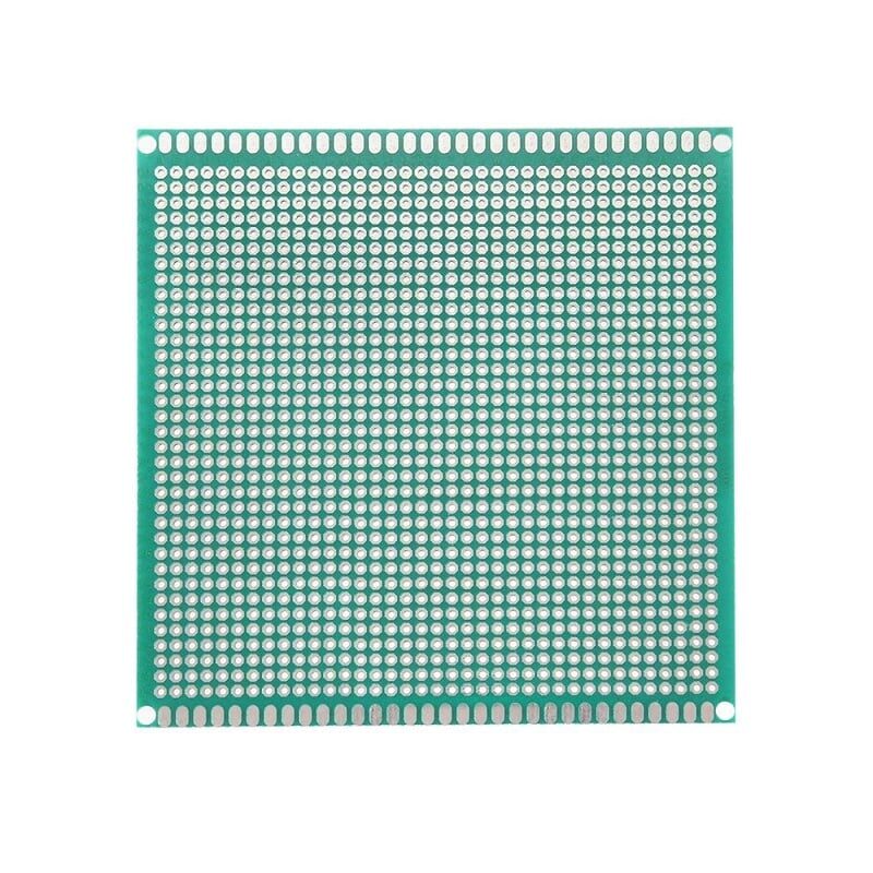
10 x 10 cm Universal PCB Prototype Board
Once you’ve verified your BJT bias circuit on a breadboard, transfer it to this universal PCB for a permanent, reliable amplifier. The 2.54mm pitch fits all standard through-hole components.
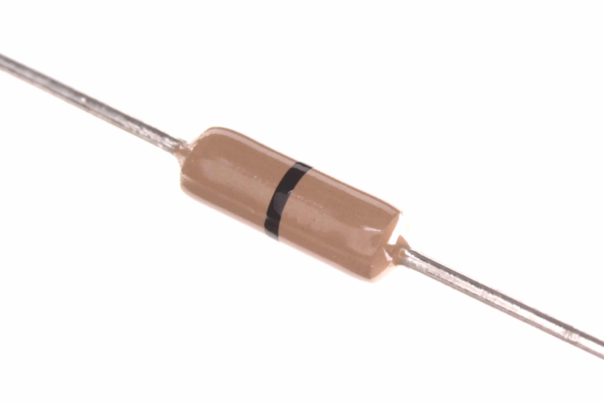
10 Ohm 0.25W Carbon Film Resistor (Pack of 50)
Carbon film resistors with ±5% tolerance are perfect for BJT biasing circuits. Stock up on multiple values to build your resistor kit and experiment with different Q-point settings.
Frequently Asked Questions
Why is voltage divider bias the most commonly used BJT biasing method?
Voltage divider bias is preferred because it makes the Q-point nearly independent of the transistor’s current gain β. Since β varies widely even between transistors of the same part number, a bias circuit that doesn’t rely on β gives consistent performance. The rule of thumb — make the divider current 10× the base current — ensures the Thevenin voltage at the base is stiff (unaffected by loading), fixing V_B and hence I_C regardless of β.
What is the purpose of the emitter resistor RE in BJT biasing?
The emitter resistor RE provides DC negative feedback that stabilises the Q-point. If temperature rises and I_C increases, the emitter voltage V_E = I_E × RE also increases. Since V_B is held fixed by the voltage divider, V_BE = V_B − V_E decreases, reducing base current and hence collector current — counteracting the original increase. For AC signals, RE is bypassed by a capacitor to prevent it from reducing voltage gain.
What happens if the BJT is biased in saturation instead of the active region?
In saturation, V_CE drops to a very low value (typically 0.1–0.2V for a saturated BJT). The transistor acts like a closed switch and cannot amplify AC signals — any AC signal applied will be clipped or severely distorted. Saturation is intentional for digital switching but a design error for linear amplification. To move back to the active region, reduce the base drive (increase RB) or reduce the collector load (decrease RC).
How do I measure the Q-point of a BJT amplifier circuit?
Use a digital multimeter. First, measure V_C (collector to ground) and V_E (emitter to ground). Then V_CE = V_C − V_E. To find I_C, measure the voltage drop across RC: I_C = V_RC / RC = (V_CC − V_C) / RC. Compare these measured values against your design calculations to verify correct biasing. If V_CE is near 0V, the transistor is saturated; if near V_CC, it is cut off.
Can I use PNP transistors with the same biasing methods?
Yes, all four biasing methods work for PNP transistors, but the polarities are reversed. The supply voltage VCC becomes a negative supply (or the circuit is inverted). In voltage divider bias for a PNP transistor, the base voltage must be lower than the emitter voltage (V_B < V_E) with V_EB ≈ 0.7V. Current flows from emitter to collector (conventional current direction is reversed compared to NPN). Many textbooks illustrate NPN circuits; simply mirror the supply voltages for PNP.
Build Your BJT Amplifier Today
Get BC547, 2N2222, resistors, capacitors, and prototype PCBs from Zbotic — everything you need to design and test all BJT biasing configurations at home.


Add comment