
Whether you are a student just entering the world of electronics or a seasoned hobbyist building your tenth Arduino project, mastering the electronic symbols quiz is a rite of passage every maker must face. Schematic symbols are the universal language of electronics — the alphabet that lets engineers and hobbyists across India and the world communicate circuit ideas without ambiguity. In this guide, we will test your knowledge, explain the most important symbols, and give you the tools to read any circuit diagram with confidence.
Why Electronic Symbols Matter
Imagine trying to describe a circuit using only words: “Connect a 10 kilo-ohm resistor to the positive supply rail, then add a 0.1 microfarad capacitor to ground, followed by an NPN transistor with its base driven by a 1 kilo-ohm resistor…” It becomes unwieldy very quickly. Schematic symbols replace all of that with clean, compact, internationally recognised graphical shorthand.
In India, electronics education follows both IEC (International Electrotechnical Commission) and IEEE/ANSI standards. Most textbooks — NCERT, CBSE board material, and university syllabi — use a mixture of both. Understanding both sets of symbols ensures you can read a European datasheet as fluently as an American application note.
Beyond academic value, symbol literacy is practically essential. When you buy an op-amp IC, the datasheet will show a triangle with input pins — if you do not know what that means, you cannot wire it up. When you troubleshoot a PCB, you need to trace the schematic and identify every component. Symbol knowledge is the bridge between a parts list and a working circuit.
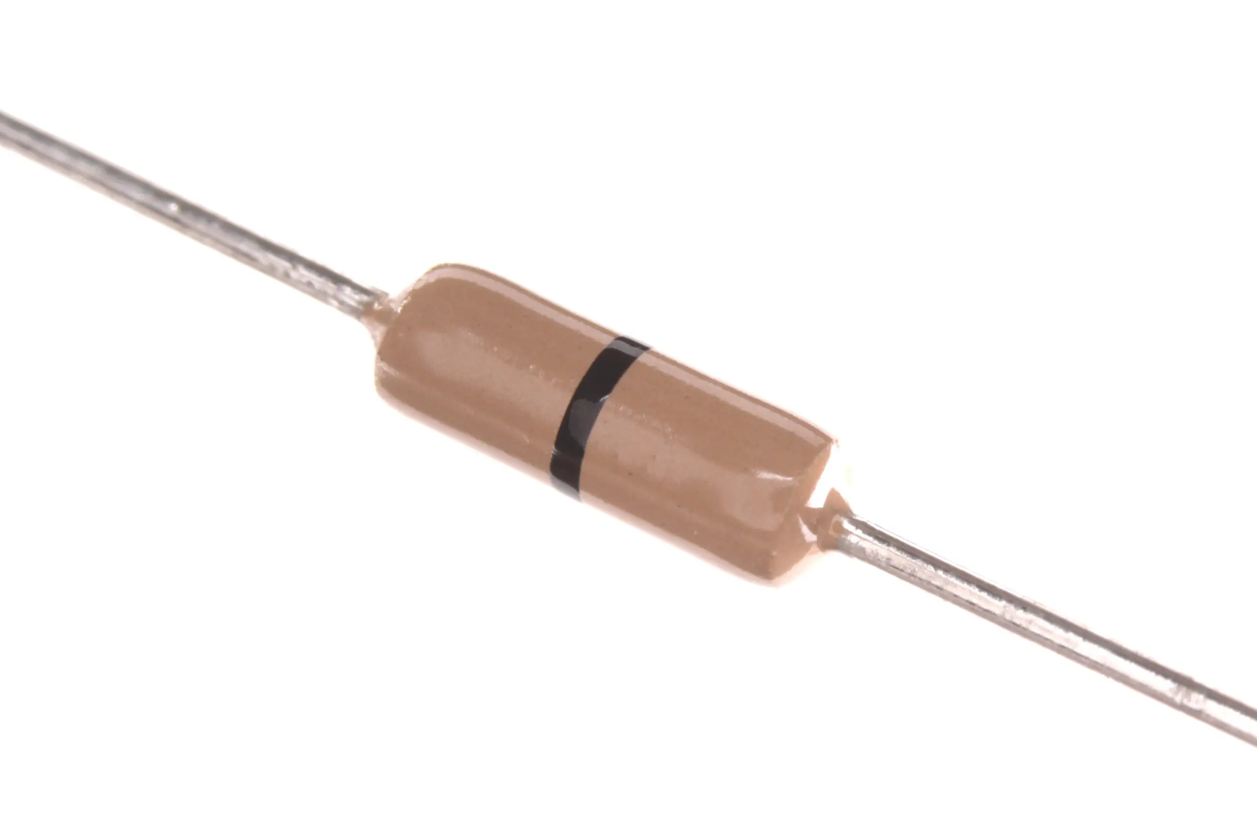
0 Ohm 0.25W Carbon Film Resistor (Pack of 100)
Perfect for beginners learning resistor symbols — practice reading colour bands and understand how 0-ohm jumpers work in schematics.
Passive Component Symbols
Passive components do not amplify or switch — they resist, store, or release energy. These are the most common symbols you will encounter in any schematic.
Resistor
The resistor is represented in two ways: the IEEE/ANSI standard uses a zigzag line (resembling a zig-zag wave), while the IEC standard uses a plain rectangle. In India, both appear in textbooks. The unit is Ohm (Ω), and resistors control current flow. Colour bands tell you the value: for a 4-band resistor, the first two bands are digits, the third is the multiplier, and the fourth is tolerance. A resistor with bands Brown–Black–Orange–Gold reads: 10 × 1000 = 10 kΩ, ±5%.
Capacitor
The capacitor symbol shows two parallel lines (plates). A polarised capacitor (electrolytic) has a curved line for the negative plate or a plus sign near the positive lead. Non-polarised capacitors use two straight parallel lines. Capacitance is measured in Farads (F), though most practical values are in microfarads (µF), nanofarads (nF), or picofarads (pF). Capacitors store energy in an electric field and are used for filtering, coupling, and timing circuits.
Inductor
An inductor is shown as a series of bumps or loops, representing wire coiled into a solenoid. The IEC version uses a rectangle. Inductance is measured in Henries (H). Inductors oppose changes in current and are used in filters, oscillators, and power supplies.
Diode
A diode symbol is a triangle pointing at a vertical bar — the triangle is the anode (positive), and the bar is the cathode (negative). Current flows in the direction the triangle points. Variants include: Zener diode (bent bar — used for voltage regulation), LED (triangle/bar with two arrows pointing outward — represents light emission), and Schottky diode (an S-shaped bar for low forward voltage drop).
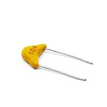
0.1/100nF TH-Multilayer Ceramic Capacitor (Pack of 50)
The ubiquitous 100nF decoupling capacitor — every schematic has one. Stock up and learn exactly where and why they appear on circuit diagrams.
Active Component Symbols
Active components require an external power source and can amplify signals. These symbols take a bit more study but are equally essential.
Bipolar Junction Transistor (BJT)
A BJT has three terminals: Base (B), Collector (C), and Emitter (E). The NPN transistor symbol shows an arrow on the emitter pointing outward (away from the base line), while the PNP has the arrow pointing inward. A useful mnemonic: NPN = “Not Pointing iN”. BJTs are used as switches and amplifiers. In India, the BC547 (NPN) and BC557 (PNP) are the most commonly found in hobby kits.
MOSFET
The MOSFET (Metal Oxide Semiconductor Field Effect Transistor) symbol shows three terminals: Gate (G), Drain (D), and Source (S). N-channel MOSFETs have an arrow pointing inward on the body diode; P-channel arrows point outward. The broken line between gate and channel represents the insulating oxide layer. MOSFETs are preferred for power switching due to their high input impedance and fast switching speed.
Operational Amplifier (Op-Amp)
The op-amp is drawn as a triangle with two inputs on the left (inverting: marked −, non-inverting: marked +) and one output on the right. Power supply pins (V+ and V−) are usually omitted from simplified schematics. Op-amps are the workhorses of analog electronics — used for amplification, filtering, comparison, and mathematical operations. The LM741, LM358, and TL071 are classics available at most Indian electronics shops.
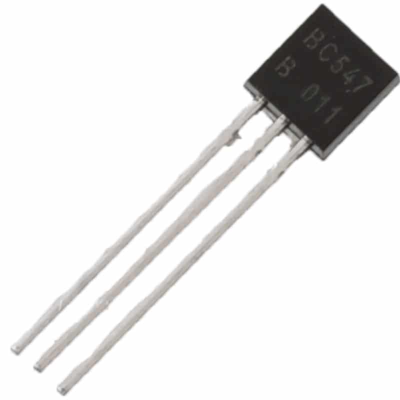
BC547 NPN 100mA Transistor TO-92 (Pack of 10)
The classic NPN transistor used in millions of hobby projects. Recognise its schematic symbol and build your first amplifier or switch circuit today.
Power and Ground Symbols
Power and ground symbols anchor every schematic. Without them, you cannot determine voltage references or supply rails.
- VCC / VDD / V+: An upward-pointing arrow or a horizontal line labelled with the voltage (e.g., +5V, +12V). VCC is used for BJT circuits; VDD is used for MOSFET/CMOS circuits.
- Ground (GND): Three horizontal lines of decreasing length stacked below a vertical line. Earth ground uses a diagonal line pattern instead. Signal ground (chassis ground) uses a triangle pointing downward.
- Battery: Alternating long and short horizontal lines — long lines are positive plates, short lines are negative. The total voltage is the sum of all cells.
- Power Flag: A flag-shaped symbol indicating a net that is explicitly connected to power — used in EDA tools like KiCad to prevent ERC warnings.
Logic Gate Symbols
Digital electronics uses logic gate symbols to represent Boolean operations. The IEEE/ANSI symbols are the most widely used:
- AND gate: D-shaped body with a flat left side — output is HIGH only when ALL inputs are HIGH.
- OR gate: Curved shield shape — output is HIGH when ANY input is HIGH.
- NOT gate (Inverter): Triangle with a bubble at the output — inverts the logic level.
- NAND gate: AND gate with an output bubble — universal gate, can implement any logic function.
- NOR gate: OR gate with an output bubble — also a universal gate.
- XOR gate: OR gate with an extra curved line at the input — output HIGH when inputs are different.
- XNOR gate: XOR gate with an output bubble — output HIGH when inputs are the same.
The IEC rectangular symbol standard replaces the organic shapes with rectangles labelled &, ≥1, =1, etc. This style appears in European datasheets and some Indian university textbooks.
The Electronic Symbols Quiz
Test yourself on these 10 questions. Try to answer before checking the answers section below!
- A zigzag line on a schematic (ANSI standard) represents which component?
- Two parallel plates — one curved — represent what type of capacitor?
- A triangle pointing at a bar represents which component? What does the bar represent?
- Which transistor type has its emitter arrow pointing outward?
- A triangle with a minus sign (−) on the left and plus (+) below it represents which IC?
- Three stacked horizontal lines of decreasing width below a node represent what?
- An OR-gate shape with a bubble at the output is which logic gate?
- A loop of bumps (or semicircles) in a schematic represents which passive component?
- A Zener diode differs from a standard diode symbol by having a _____ at the cathode bar.
- The letter M with a broken middle line and three terminals represents which component?
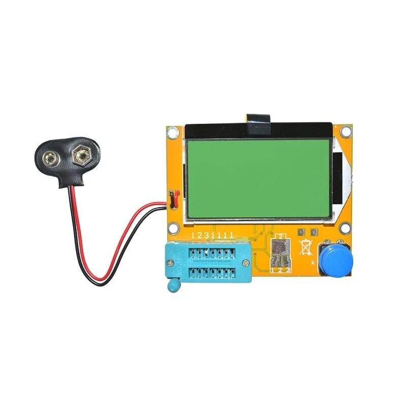
LCR-T4 LCD Graphical Transistor Tester – Resistance, Capacitance, ESR, SCR
Identify unknown components automatically — this tester displays the component type and schematic symbol on screen. Great learning tool for anyone studying electronics symbols.
Quiz Answers and Explanations
- Resistor. The zigzag (ANSI) symbol is the most recognisable passive component symbol in American and Indian textbooks. The IEC equivalent is a rectangle.
- Polarised (electrolytic) capacitor. The curved plate is always the negative terminal. Always observe polarity when placing electrolytic capacitors in a circuit — reversing them can cause catastrophic failure.
- Diode. The bar represents the cathode (negative terminal). Current flows from anode (triangle tip) to cathode (bar), but conventional current flows from + to −, so the triangle points in the direction of conventional current flow.
- NPN transistor. Memory aid: NPN = “Not Pointing iN.” The PNP emitter arrow points inward toward the base.
- Operational amplifier (op-amp). The − input is the inverting input and the + input is the non-inverting input. Many schematics omit the power supply pins for clarity.
- Ground (GND). This is the most common ground symbol. Earth ground uses angled diagonal lines, and chassis/signal ground uses a triangle.
- NOR gate. NOR = NOT + OR. The bubble negates the OR gate output. NOR is a universal gate — you can build any logic circuit using only NOR gates.
- Inductor. The bumps represent coil windings. A core line underneath the bumps indicates a ferromagnetic core (higher inductance).
- Bent ends (Z-shape). The bent cathode bar on a Zener diode indicates it is designed to conduct in reverse breakdown at a specific voltage (the Zener voltage), making it ideal for voltage regulation.
- MOSFET. The broken gate line represents the insulated gate. The three terminals are Gate, Drain, and Source. The arrow direction on the body indicates N-channel or P-channel.
Score Guide: 9–10 correct: You are a schematic expert! 6–8: Solid foundation — keep practising with real schematics. 3–5: Review the passive and active component sections above and try again. 0–2: Start with a beginner electronics kit and study each component before moving to schematics.
Frequently Asked Questions
What is the difference between IEEE and IEC electronic symbols?
IEEE/ANSI symbols (common in the USA and India) use organic shapes — zigzags for resistors, organic curves for gate symbols. IEC symbols (common in Europe) use rectangles for resistors and labelled rectangles for logic gates. Both are correct; knowing both helps you read international datasheets.
Where can I practice reading schematics?
Excellent free resources include CircuitLab, EasyEDA, and Falstad Circuit Simulator. SparkFun and Adafruit also publish beginner schematic tutorials. The best practice is to pick up a real schematic (a classic 555 timer circuit is a great start) and trace every symbol manually.
Are electronic symbols the same worldwide?
The core symbols are nearly universal, but there are regional differences — particularly for resistors (zigzag vs rectangle) and some sensor symbols. Datasheets from Japanese manufacturers sometimes use JIS symbols which differ slightly. For global work, familiarise yourself with both IEEE and IEC standards.
How do I remember all the transistor symbols?
Use mnemonics: for NPN, “Not Pointing iN” (arrow points away from base line). For PNP, “Pointing iN Please” (arrow points toward base line). For MOSFETs, remember that the gate is always isolated (shown by a gap in the symbol), distinguishing it from BJTs.
Which software is best for drawing circuit schematics in India?
KiCad (free, open-source) is the most popular choice for students and professionals. EasyEDA (free, browser-based) integrates with JLCPCB for PCB manufacturing. Altium Designer and OrCAD are professional tools used in industry. For quick sketches, CircuitLab and Circuit Diagram (web app) work without installation.
Now that you can read a schematic, it is time to put components on a breadboard! Zbotic stocks a wide range of resistors, capacitors, transistors, ICs, and prototyping tools for Indian makers. Explore the Electronics Basics collection and start building today.


Add comment