
In the real world, sensor signals are messy. A thermocouple outputs millivolts with noise riding on top. A pressure sensor’s zero output drifts with temperature. A photodiode current is tiny and buried in 50 Hz hum from fluorescent lighting. Before any microcontroller ADC can make sense of these signals, they must be cleaned up — this process is called signal conditioning. This tutorial covers everything you need to know about signal conditioning: amplification, filtering, and offset removal, with practical circuit examples you can build today.
What Is Signal Conditioning?
Signal conditioning is the process of manipulating a raw sensor signal to make it suitable for the next stage in the signal chain — typically an ADC (Analog-to-Digital Converter) in a microcontroller. A raw signal may have one or more of these problems:
- Wrong amplitude: The signal is too weak (e.g., 0–50 mV from a thermocouple) or too strong (e.g., a 0–10V industrial sensor feeding a 3.3V ADC).
- DC offset: The signal rides on a non-zero baseline (e.g., a bridge sensor that outputs 2.5V ± 0.1V instead of 0–5V).
- Noise and interference: High-frequency switching noise, 50 Hz power line hum, or radio frequency interference rides on the signal.
- Wrong impedance: The sensor cannot drive the load directly without loading effects causing measurement errors.
- Non-linearity: Some sensors have a non-linear transfer function that needs linearisation before the ADC sees a useful signal.
A signal conditioning circuit addresses these issues using amplifiers, filters, and level-shifting circuits — almost always built around operational amplifiers (op-amps).
Amplification: Boosting Weak Signals
The first step for most sensor signals is amplification. Op-amps configured as inverting or non-inverting amplifiers are the standard choice.
Non-Inverting Amplifier
The non-inverting amplifier has the signal at the + (non-inverting) input and a feedback network at the − (inverting) input. The voltage gain is:
Av = 1 + (Rf / R1)
where Rf is the feedback resistor and R1 is the resistor from the inverting input to ground. The key advantage of the non-inverting configuration is very high input impedance — it barely loads the source. For example, with Rf = 9 kΩ and R1 = 1 kΩ, you get a gain of 10×. A 50 mV thermocouple signal becomes 500 mV — within a useful ADC range.
Inverting Amplifier
The inverting amplifier places the signal at the − input through a resistor Rin, with a feedback resistor Rf from output to −. The gain is:
Av = −(Rf / Rin)
The negative sign means the output is phase-inverted (180° flip). Input impedance is equal to Rin. For a gain of −10×, use Rf = 10 kΩ and Rin = 1 kΩ. The inverting configuration is preferred when you need a precise gain and the signal source has low impedance.
Instrumentation Amplifier
When the sensor signal is differential (two wires, neither grounded) — as in Wheatstone bridge sensors, thermocouples, and ECG electrodes — a standard op-amp cannot reject common-mode noise efficiently. The instrumentation amplifier (INA) uses three op-amps in a configuration that provides high common-mode rejection ratio (CMRR, typically >80 dB), high differential gain, and high input impedance. ICs like the INA128, INA333, and AD620 integrate all three op-amps with a single external resistor for gain setting. The gain formula for most INA ICs is:
Av = 1 + (50 kΩ / Rg) (for INA128)
For a gain of 100, use Rg = 505 Ω (use 499 Ω standard value).
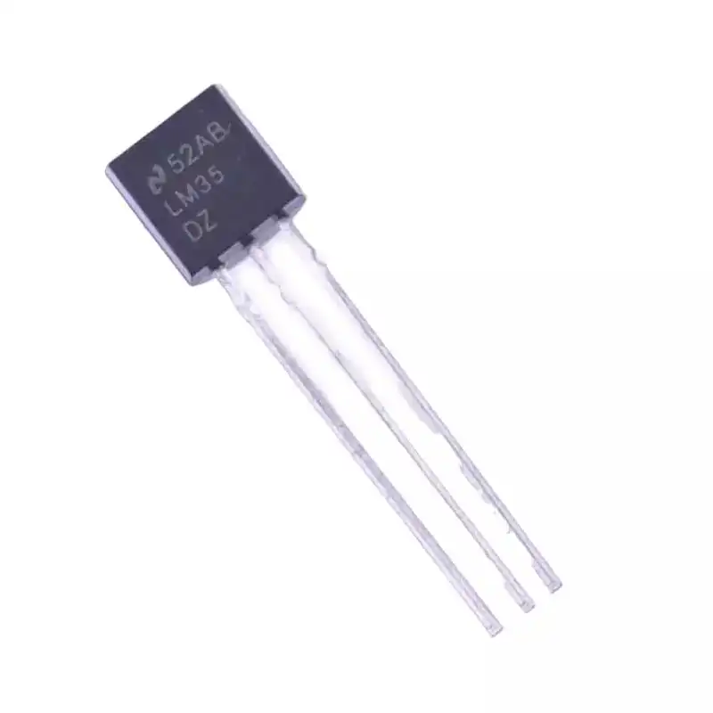
LM35 Temperature Sensor
Output 10mV/°C — a perfect low-level signal to practice amplification and level-shifting on. Accurate, reliable, and widely used in Indian engineering labs.
Filtering: Removing Noise
After amplification, noise that was small before amplification is now also amplified. Filtering removes unwanted frequency components while preserving the signal of interest.
Low-Pass Filter (LPF)
A low-pass filter allows low frequencies to pass and attenuates high frequencies. For sensor signals (which are inherently slow-moving physical quantities like temperature, pressure, and humidity), a low-pass filter is the most common choice. The simplest is an RC LPF:
- Cutoff frequency: fc = 1 / (2π × R × C)
- For fc = 100 Hz: use R = 15.9 kΩ (use 16 kΩ) and C = 0.1 µF
Above fc, the filter attenuates at −20 dB/decade (first order). For steeper roll-off, use second-order or Sallen-Key active filters built around op-amps — these achieve −40 dB/decade without using inductors.
High-Pass Filter (HPF)
High-pass filters block DC and low frequencies while allowing high frequencies through. They are used for AC-coupling — removing a DC bias while passing the AC signal. In audio amplifiers and ECG circuits, HPFs block the DC operating point from reaching subsequent stages. The RC HPF cutoff is the same formula as LPF, but R and C are swapped in position.
Band-Pass Filter
A band-pass filter passes a range of frequencies centred on a centre frequency (f0) and attenuates frequencies above and below. They are used in ultrasonic sensors, radio receivers, and vibration analysis where only a specific frequency band carries useful information.
Notch Filter (Band-Stop Filter)
In India, power lines operate at 50 Hz. Any sensor near electrical wiring will pick up 50 Hz interference. A notch filter (also called a band-stop or band-reject filter) attenuates a narrow frequency band — specifically 50 Hz — while passing everything else. The Twin-T notch filter is a classic op-amp-based circuit for this purpose. Set the component values so that 2πf0RC = 1 for the notch frequency.

0.1µF 50V Capacitor (Pack of 50)
Essential for building RC low-pass filters in your signal conditioning circuits. Also doubles as a decoupling capacitor on your op-amp power supply pins.
Offset Removal and Level Shifting
Many sensors output a signal with a DC offset — a non-zero voltage when the measured quantity is zero. For example, a 4–20 mA current loop sensor connected through a 250 Ω resistor outputs 1V (at zero/minimum) to 5V (at maximum). To use the full ADC range, you need to shift the 1–5V range down to 0–4V (level shifting) or subtract the 1V offset.
Summing Amplifier for Offset Subtraction
The op-amp summing (inverting) amplifier can add a precision negative reference voltage to the signal, effectively subtracting the offset. The output is:
Vout = −Rf × (Vin1/R1 + Vin2/R2)
If Vin1 is your signal (with offset) and Vin2 is a precision negative reference equal to the offset, the two terms cancel — the output is offset-free. A TL431 adjustable shunt reference or a simple resistor divider from a stable supply provides the reference voltage.
Difference Amplifier for Offset Rejection
A difference amplifier subtracts two signals. If one input is your signal and the other is a precision reference set to the expected offset, the output is only the signal variation. With matched resistors (R1=R2=R3=R4=R), the gain is 1× and the circuit perfectly rejects common-mode voltages including the offset.
Rail-to-Rail Op-Amps for 3.3V Systems
When working with 3.3V microcontrollers (ESP32, STM32, nRF52), use rail-to-rail op-amps (MCP6001, LMV321, OPA314) that can swing output voltage all the way from 0V to 3.3V. Standard op-amps like LM358 cannot reach within 1–1.5V of the supply rail, wasting precious ADC range.
Building a Complete Signal Conditioning Chain
A complete signal conditioning chain typically has these stages in order:
- Input protection: Transient voltage suppressors (TVS diodes) or series resistors protect the op-amp from voltage spikes from long sensor cables.
- Buffering / Impedance matching: A unity-gain buffer (voltage follower) presents high impedance to the sensor and low impedance to the next stage — preventing loading effects.
- Amplification: Bring the signal up to a useful ADC range (typically 0–3.3V or 0–5V).
- Offset removal / Level shifting: Shift the amplified signal’s baseline to 0V (or to the ADC’s midpoint for bipolar signals).
- Filtering: Low-pass filter set just above the maximum signal frequency to reject noise and prevent aliasing. The cutoff must be at or below the Nyquist frequency (half the ADC sampling rate).
- Anti-aliasing: A final RC filter immediately before the ADC input to hard-limit the signal bandwidth — prevents high-frequency noise from folding into the baseband during sampling.
Practical Example: LM35 Temperature Sensor
The LM35 outputs 10 mV/°C with 0 mV at 0°C. For a measurement range of 0–100°C, the output is 0–1V. To use a 0–3.3V ADC efficiently, you need a gain of 3.3× and ideally some filtering.
Circuit design:
- Non-inverting amplifier with Av = 3.3: Use Rf = 23 kΩ and R1 = 10 kΩ (gives Av = 1 + 23/10 = 3.3). Standard values: 22 kΩ + 1 kΩ in series for Rf, R1 = 10 kΩ.
- Low-pass filter after the amplifier: fc = 10 Hz (since temperature changes slowly). R = 16 kΩ, C = 1 µF electrolytic.
- Place 100 nF decoupling capacitors on the LM35’s supply pin and on the op-amp’s V+ and V− pins to GND.
- Result: 0°C → 0V, 100°C → 3.3V — full ADC range used, noise-free readings.
This is exactly the kind of signal conditioning chain used in professional data loggers, industrial temperature controllers, and IoT sensor nodes built across India’s maker community.
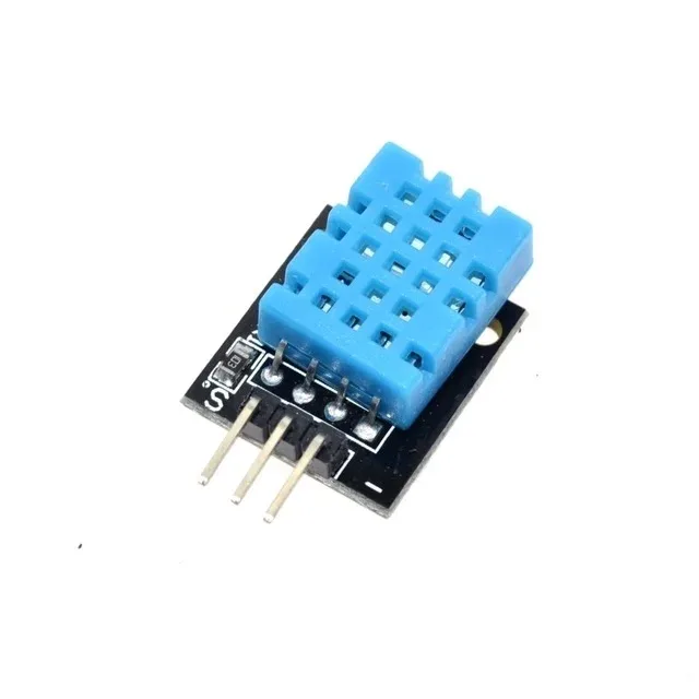
DHT11 Digital Humidity and Temperature Sensor Module
After mastering analog signal conditioning with LM35, explore digital sensor protocols with the DHT11 — understanding both analog and digital sensor interfaces is essential for modern makers.
Common Mistakes and How to Avoid Them
- Forgetting op-amp power supply decoupling: Always place a 100 nF ceramic capacitor between each power supply pin (V+ and V−) and ground, as close to the IC as possible. Switching noise on the supply rail couples directly into the op-amp output.
- Setting gain too high in one stage: If you need a gain of 1000×, use two stages of 31.6× each (cascaded amplifiers) rather than one stage of 1000×. High single-stage gain severely limits bandwidth and increases output offset due to input bias currents.
- Ignoring op-amp bandwidth: Every op-amp has a gain-bandwidth product (GBP). An LM358 has a GBP of ~1 MHz. At a gain of 100×, the −3dB bandwidth is only 10 kHz. For higher-frequency signals, use a faster op-amp (TL072, OPA2134, AD8620).
- Not accounting for common-mode input range: For single-supply op-amps, the inputs must stay within the common-mode input voltage range — typically 0V to (VCC − 1.5V). Signals that touch the supply rail will clip. Use rail-to-rail op-amps (MCP6002, LMV358) to avoid this issue.
- Floating inputs: Never leave an op-amp input unconnected. Floating inputs pick up noise and can drive the output to saturation. Connect unused inputs through a resistor to GND or to a defined voltage.
Frequently Asked Questions
What is the difference between signal conditioning and signal processing?
Signal conditioning is analog — it happens before the ADC, using physical components to prepare the signal. Signal processing is typically digital — it happens after the ADC, using algorithms (FFT, digital filters, etc.) in a microcontroller or DSP. Both are often needed in a complete measurement system.
Can I use an Arduino’s built-in ADC without signal conditioning?
For simple sensors with well-matched output ranges (like many module-format sensors), yes. But for precision measurements, small sensor outputs (thermocouples, strain gauges, pH probes), or noisy environments, signal conditioning is essential. The Arduino ADC has only 10-bit resolution (1024 counts over 5V = ~4.9 mV per count) — without amplification, a 50 mV sensor signal would give you only ~10 counts of resolution.
What op-amp should I use for signal conditioning at 3.3V?
For single-supply 3.3V systems, use rail-to-rail op-amps: MCP6001/MCP6002 (very low cost, excellent for hobbyists), LMV321/LMV358, or OPA314. These can swing output voltage from near 0V to near 3.3V, maximising ADC utilisation.
How do I remove 50 Hz hum from a sensor signal in India?
Use a Twin-T notch filter designed for 50 Hz. Alternatively, use differential measurement (instrumentation amplifier) which rejects common-mode 50 Hz pickup. Shielded cables and proper grounding also dramatically reduce hum pickup before it even reaches your conditioning circuit.
What is an anti-aliasing filter and why does it matter?
An anti-aliasing filter is a low-pass filter placed directly before the ADC input. Its cutoff frequency must be set to ≤ fs/2 (where fs is the ADC sampling rate) to prevent high-frequency components from being “aliased” (incorrectly appearing as low-frequency signals in the digital domain). Without it, high-frequency noise appears as false low-frequency signal components in your measurement.
Ready to go hands-on? Zbotic stocks all the components you need — resistors, capacitors, op-amp ICs, and sensors — delivered fast to your door across India. Visit our Electronics Basics store and build your first precision measurement circuit today.


Add comment