
The operational amplifier — or op-amp — is one of the most versatile building blocks in analogue electronics. A single op-amp IC can amplify signals, sum voltages, differentiate waveforms, compare levels, filter noise, and generate oscillations. But before you can exploit all that versatility, you need to master the two foundational configurations: the inverting amplifier and the non-inverting amplifier.
In this guide we cover both configurations in depth — their circuit diagrams, gain formulas, input/output impedances, worked numerical examples, and practical design considerations. Whether you are a student, a hobbyist, or an engineer refreshing your fundamentals, you will find everything you need here.
The Ideal Op-Amp: Key Properties
An ideal op-amp has three defining properties that make the gain formulas simple and elegant:
- Infinite open-loop gain (A_ol → ∞): The open-loop voltage gain is extremely high (typically 100,000 or more in real devices). In closed-loop configurations, this makes the closed-loop gain depend only on the external resistors, not on the op-amp itself.
- Infinite input impedance: No current flows into either input terminal (V+ or V−). This means the input resistors carry all the current without any going into the op-amp.
- Zero output impedance: The output can source or sink current without any voltage drop — it is a perfect voltage source.
- Infinite bandwidth: Ideal op-amps amplify all frequencies equally. Real op-amps have a finite gain-bandwidth product (GBW).
Virtual Ground and Virtual Short Concepts
These two concepts are the keys to deriving all op-amp circuit behaviour quickly:
Virtual Short
Because A_ol is infinite and the output is finite, the differential input voltage (V+ − V−) must be essentially zero in any stable negative-feedback circuit. Therefore:
V+ ≈ V− (virtual short between the two input terminals)
The inputs are not shorted — no current flows between them — but their voltages are equal.
Virtual Ground
In the inverting amplifier, the non-inverting input (V+) is connected to ground (0 V). Because of the virtual short, V− also equals 0 V. This point (the inverting input) is therefore at virtual ground — it sits at 0 V without being physically connected to ground.
Inverting Amplifier Circuit
The inverting amplifier uses negative feedback through a resistor from the output back to the inverting (−) input:
- Input signal V_in → R_in → inverting input (−)
- Feedback resistor R_f from output → inverting input (−)
- Non-inverting input (+) → Ground (via a bias compensation resistor R_bias = R_in ‖ R_f)
The R_bias at V+ is technically optional (for ideal op-amps) but good practice in real circuits to balance the bias current offset.
Inverting Amplifier Gain Formula and Derivation
Derivation Using Virtual Ground
Since V+ = 0 V and (virtual short) V− = V+ = 0 V:
Current through R_in: I₁ = (V_in − V−) / R_in = V_in / R_in

Since no current enters the op-amp input, all of I₁ flows through R_f:
I₁ = (V− − V_out) / R_f = −V_out / R_f

Equating:
V_in / R_in = −V_out / R_f

Therefore:
A_v = V_out / V_in = −R_f / R_in
Key Points
- Gain magnitude = R_f / R_in
- The negative sign means 180° phase inversion
- Gain depends only on resistor ratio — not on the op-amp’s own gain
- To set a gain of −10: R_f = 10 × R_in (e.g. R_in = 10 kΩ, R_f = 100 kΩ)
Input and Output Impedance (Inverting)
Z_in = R_in  (because V− is at virtual ground, the input signal sees R_in to ground)
Z_out ≈ 0 Ω  (ideal; real op-amps: Z_out = Z_out_open / (1 + A_ol × β) → very small)
Note: The input impedance of the inverting configuration is simply R_in, which may be too low for high-impedance sources. This is a key disadvantage compared to the non-inverting configuration.
Inverting Amplifier Worked Example
Design a −20 dB inverting amplifier (gain = −10) with input impedance of 10 kΩ:
Given: A_v = −10, Z_in = 10 kΩ

Step 1: R_in = Z_in = 10 kΩ
Step 2: R_f = |A_v| × R_in = 10 × 10k = 100 kΩ
Step 3: R_bias = R_in ‖ R_f = (10k × 100k) / (10k + 100k) = 9.09 kΩ → use 9.1 kΩ

Verification: A_v = −R_f/R_in = −100k/10k = −10 ✓
Finding output voltage for a given input:
V_in = 0.5 V (peak)
V_out = A_v × V_in = −10 × 0.5 = −5 V (peak)

Note: V_out cannot exceed the supply rails (e.g. ±12 V supply → V_out max ≈ ±10 V for typical op-amps)
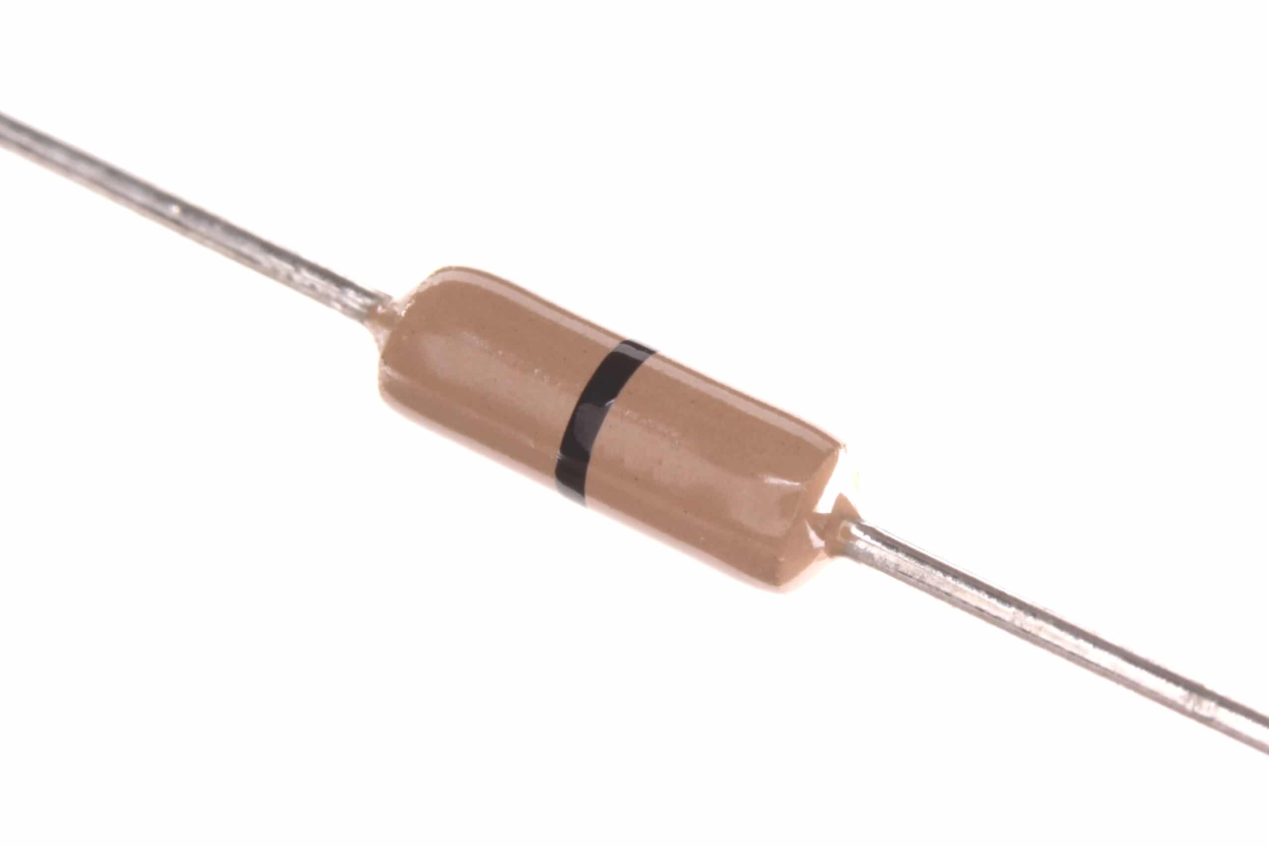
0 Ohm 0.25W Carbon Film Resistors (Pack of 100)
Build op-amp circuits with accurate resistor ratios — 1% metal film resistors give you precise gain setting for both inverting and non-inverting configurations.
Non-Inverting Amplifier Circuit
The non-inverting amplifier applies the input signal to the non-inverting (+) input and uses feedback from the output to the inverting (−) input through a resistor divider:
- Input signal V_in → non-inverting input (+)
- R₁ from inverting input (−) → Ground
- R_f from output → inverting input (−)
- This forms a voltage divider that sets the feedback fraction β = R₁/(R₁ + R_f)
Non-Inverting Amplifier Gain Formula and Derivation
Derivation Using Virtual Short
V+ = V_in
Virtual short: V− = V+ = V_in

V− is set by the voltage divider (R₁ and R_f):
V− = V_out × R₁ / (R₁ + R_f)

Equating:
V_in = V_out × R₁ / (R₁ + R_f)

Therefore:
A_v = V_out / V_in = 1 + R_f / R₁
Key Points
- Gain is always greater than or equal to 1
- No phase inversion (output in phase with input)
- When R_f = 0 (short) and R₁ = ∞ (open): A_v = 1 (voltage follower)
- To set A_v = 11: R_f = 10 × R₁ (e.g. R₁ = 10 kΩ, R_f = 100 kΩ)
Input and Output Impedance (Non-Inverting)
Z_in = Z_in_open_loop / (1 + A_ol × β) → extremely high (gigaohms for ideal)
Z_out ≈ 0 Ω (same as inverting — feedback reduces output impedance)
This extremely high input impedance is the primary advantage of the non-inverting configuration — it draws virtually no current from the signal source.
Non-Inverting Amplifier Worked Example
Design a non-inverting amplifier with gain = +11 (approximately +20.8 dB):
Given: A_v = 11

1 + R_f/R₁ = 11 → R_f/R₁ = 10

Choose R₁ = 10 kΩ → R_f = 100 kΩ

Verification: A_v = 1 + 100k/10k = 11 ✓
Output for a 100 mV input:
V_out = 11 × 100 mV = 1.1 V (same phase as input)
Bandwidth check (assuming LM741 with GBW = 1 MHz):
f_-3dB = GBW / A_v = 1 MHz / 11 ≈ 91 kHz
(This means the amplifier works flat up to ~91 kHz at this gain)
Voltage Follower (Unity Gain Buffer)
The voltage follower is a special case of the non-inverting amplifier with R_f = 0 and R₁ = ∞:
A_v = 1 + 0/∞ = 1
V_out = V_in (exactly, in phase)
While it might seem useless to have a gain of 1, the voltage follower is extremely valuable as an impedance buffer:
- Takes a high-impedance signal (e.g. from a sensor) and presents it as a low-impedance output capable of driving a load without loading the source.
- Used between a voltage divider and a load to prevent the load from disturbing the divider ratio.
- Prevents sensor output from being loaded by a low-impedance ADC input.
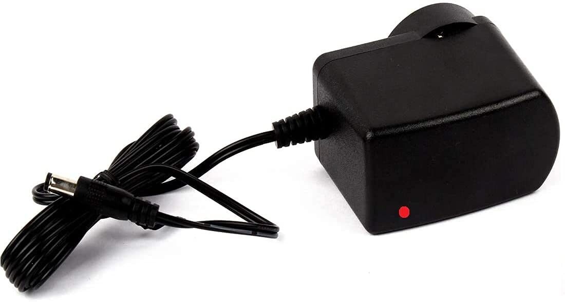
12V 2A Power Supply with 5.5mm DC Plug Adapter
Power your op-amp breadboard circuits with this stable 12V DC supply — op-amps like the LM741 and TL071 require a dual supply (use a DC-DC converter for split ±12V) or single supply operation.
Inverting vs Non-Inverting: Which to Choose?
| Property | Inverting | Non-Inverting |
|---|---|---|
| Gain formula | −R_f / R_in | 1 + R_f / R₁ |
| Minimum gain | Any (including fractional) | 1 (cannot go below unity) |
| Phase | 180° inversion | In phase (0°) |
| Input impedance | = R_in (limited) | Very high (GΩ range) |
| Virtual ground | Yes (at V−) | No |
| Summing possible? | Yes (summing amplifier) | Not directly |
| Best for | Signal processing, mixers, DAC output stages | Sensor interfaces, buffers, instrumentation |
Practical Design Considerations
Resistor Value Range
Keep feedback resistors in the range of 1 kΩ to 1 MΩ. Too low a value loads the output and causes distortion; too high a value makes the circuit sensitive to parasitic capacitance and op-amp input bias current (which creates an offset voltage I_bias × R_f).
Gain-Bandwidth Product
Real op-amps have a fixed GBW. The usable bandwidth at a given closed-loop gain is:
f_-3dB = GBW / A_v
Example: TL071 GBW = 3 MHz, A_v = 100 → f_-3dB = 30 kHz
Input Bias Current Compensation
Connect a resistor R_bias = R_in ‖ R_f at the non-inverting input to V+ (to ground for inverting, to the appropriate DC potential for non-inverting). This balances the bias current offset at both inputs and minimises DC output offset.
Power Supply Decoupling
Always place 100 nF ceramic capacitors from each supply rail to ground, as close as possible to the op-amp supply pins. This is non-negotiable for stable, low-noise operation.
Output Swing Limitation
Most standard op-amps cannot swing their output all the way to the supply rails. Typical headroom is 1–2 V from each rail. Rail-to-rail op-amps (e.g. MCP6002, LMV321) can swing to within millivolts of the rails — use these for single-supply circuits.
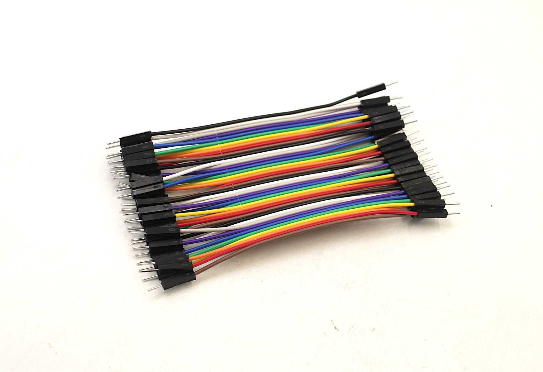
10CM Male To Male Breadboard Jumper Wires – 40Pcs
Wire up your op-amp breadboard circuits with these premium 2.54mm pitch jumper wires — essential for building and testing inverting and non-inverting amplifier configurations.
Frequently Asked Questions
What is the main difference between an inverting and non-inverting op-amp?
The main difference is where the input signal is applied. In the inverting configuration, the signal goes to the inverting (−) input, resulting in a 180° phase flip and a gain of −R_f/R_in. In the non-inverting configuration, the signal goes to the non-inverting (+) input, resulting in no phase flip and a gain of 1 + R_f/R₁. The non-inverting configuration also has a much higher input impedance.
Can the gain of an inverting op-amp be less than 1?
Yes. If R_f < R_in, the gain magnitude is less than 1 (it attenuates). For example, R_in = 100 kΩ and R_f = 10 kΩ gives A_v = −0.1. This is called an attenuating amplifier or scale factor circuit.
Why is virtual ground important?
Virtual ground is the analytical tool that makes inverting amplifier calculations simple. Because the inverting input sits at 0 V (virtual ground), the current through R_in is exactly V_in/R_in, and all of it must flow through R_f. This gives A_v = −R_f/R_in directly without needing to know A_ol.
What happens if I connect the output directly to the inverting input (no feedback resistors)?
This gives you the voltage follower (unity gain buffer). A_v = 1, no phase inversion, extremely high input impedance. The entire output is fed back, giving maximum negative feedback and hence minimum gain, maximum bandwidth, and best linearity.
Does the op-amp work with a single supply voltage?
Yes, if you use a rail-to-rail or single-supply op-amp (like LM358, MCP6002). With a single supply, you typically bias both inputs to V_CC/2 to allow signals to swing both above and below the mid-supply reference point.
How do I choose between an LM741, TL071, and LM358?
LM741: old standard, dual supply only, modest performance. TL071/TL081: JFET input (very low bias current, moderate GBW of 3 MHz), dual supply. LM358: dual op-amp, single supply, wide voltage range, but lower GBW (~1 MHz). For most modern designs, prefer LMV321 (single supply, rail-to-rail) or MCP6002 (dual, single supply, rail-to-rail, 1 MHz GBW).
Ready to Build Your Op-Amp Circuit?
Get precision resistors, a stable power supply, and jumper wires from Zbotic to build and test both inverting and non-inverting amplifier configurations on your breadboard. Seeing the gain formula work in a real circuit is the fastest way to internalise these concepts.


Add comment