
The differential amplifier op amp circuit is one of the most powerful and versatile building blocks in analog electronics. Unlike a standard amplifier that amplifies a signal referenced to ground, a differential amplifier amplifies the difference between two input signals — and ideally ignores any voltage that appears equally on both inputs (called common-mode voltage). This property makes it indispensable in sensor interfaces, audio equipment, data acquisition systems, and biomedical devices. In this guide, you will learn how to design one from scratch, understand the mathematics, and see how it is used in real-world Indian maker projects.
What Is a Differential Amplifier?
A differential amplifier has two inputs — traditionally labelled V1 and V2 — and one output. The output voltage is proportional to the difference between the two inputs:
Vout = Ad × (V2 − V1)
where Ad is the differential gain. Any voltage that appears equally on both inputs (V1 = V2 = Vcm) is called a common-mode signal. In theory, the differential amplifier completely rejects common-mode signals — in practice, it attenuates them by a factor expressed as the CMRR.
The differential amplifier concept is fundamental to many circuits you already use: the long-tailed pair in BJT amplifiers, the op-amp’s internal topology, the instrumentation amplifier in measurement equipment, and the line receiver in RS-422/RS-485 industrial communication systems. Understanding the op-amp implementation is the gateway to all of these.
Single Op-Amp Differential Amplifier
The simplest differential amplifier uses a single op-amp with four resistors. The circuit topology is:
- V1 connects through R1 to the inverting input (−) of the op-amp
- R2 connects from the inverting input to the output (feedback resistor)
- V2 connects through R3 to the non-inverting input (+)
- R4 connects from the non-inverting input to ground
Using superposition, the output voltage is:
Vout = (R2/R1) × (V2 − V1)
This equation is valid when the resistors are perfectly matched: R1 = R3 and R2 = R4. If they are matched, the gain is simply R2/R1. A common design uses:
- R1 = R3 = 10 kΩ
- R2 = R4 = 100 kΩ
- Gain = 100/10 = 10×
Input Impedance Consideration
The input impedance of the single op-amp differential amplifier is not very high — it is R1 on the inverting side and R3 + R4 on the non-inverting side. For V1, the effective input impedance is R1 (since the inverting input is a virtual ground). For V2, it is R3 + R4. If the signal source has significant source impedance, it will interact with these resistors and change the effective gain — use a buffer (voltage follower) before each input to prevent loading effects.
1.5 Ohm 1/4W Metal Film Resistor MFR (Pack of 100)
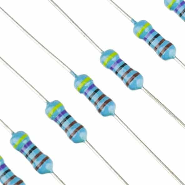
Metal film resistors with 1% tolerance are essential for differential amplifier circuits — matched resistors directly determine CMRR. Always use metal film (not carbon film) for precision analog work.
Common-Mode Rejection Ratio (CMRR)
CMRR is the measure of how well the differential amplifier rejects common-mode signals. It is defined as:
CMRR = 20 × log10(Ad / Acm)
where Ad is the differential gain and Acm is the common-mode gain (ideally zero, in practice a small non-zero value). CMRR is expressed in decibels (dB). A CMRR of 80 dB means the amplifier attenuates common-mode signals 10,000× more than differential signals.
What Limits CMRR?
In the single op-amp differential amplifier, CMRR is limited by resistor mismatch. If the four resistors are not perfectly matched, there will be a common-mode gain error. With standard 5% carbon film resistors, expect CMRR around 34 dB. With 1% metal film resistors, CMRR improves to about 46 dB. Using a precision resistor network IC (like the INA133’s internal resistors) achieves CMRR of 80+ dB.
CMRR in Practice
Consider a Wheatstone bridge strain gauge sensor. The bridge output might be 5 mV differential signal riding on a 2.5V common-mode voltage from the supply. Without high CMRR, the amplifier amplifies the 2.5V common-mode voltage along with the 5 mV signal — the 2.5V × common-mode gain completely overwhelms the tiny differential signal. With 80 dB CMRR (10,000× rejection), the 2.5V common-mode appears as only 0.25 mV at the output — negligible compared to the amplified 5 mV × 100 = 500 mV differential signal.
Three Op-Amp Instrumentation Amplifier
The three op-amp instrumentation amplifier (INA) solves the input impedance problem of the single op-amp design. It consists of two input buffer stages and one differential stage:
Stage 1: Input Buffers with Gain
Two op-amps (A1 and A2) are connected with their non-inverting inputs to V1 and V2 respectively. Their outputs feed into a resistor network. A single gain-setting resistor Rg sits between the two buffer circuits. The gain of stage 1 is:
A1 stage gain = 1 + (2R / Rg)
where R is typically 25 kΩ in standard INA ICs. This stage provides very high input impedance (essentially the open-loop input impedance of each op-amp — typically hundreds of MΩ to GΩ) and amplifies only the differential signal — common-mode signals pass through at unity gain.
Stage 2: Difference Amplifier
The second stage (op-amp A3) is a standard difference amplifier with unity gain (R3 = R4 = R5 = R6). It subtracts the two Stage 1 outputs, rejecting the common-mode component amplified by Stage 1 but preserving the differential gain. The total gain is:
Total gain = (1 + 2R/Rg)
Using Integrated INA ICs
Building a three op-amp INA from discrete components requires careful resistor matching. The practical choice is an integrated INA IC like the INA128 or INA333, which has all resistors laser-trimmed internally for excellent matching. Set the gain by connecting a single external resistor between pins 1 and 8:
| Rg (INA128) | Gain | Application |
|---|---|---|
| Open (no resistor) | 1× | Buffer / unity gain |
| 5.05 kΩ | 10× | Moderate sensor gain |
| 505 Ω | 100× | Thermocouple, bridge sensors |
| 50.5 Ω | 1000× | ECG, biomedical |
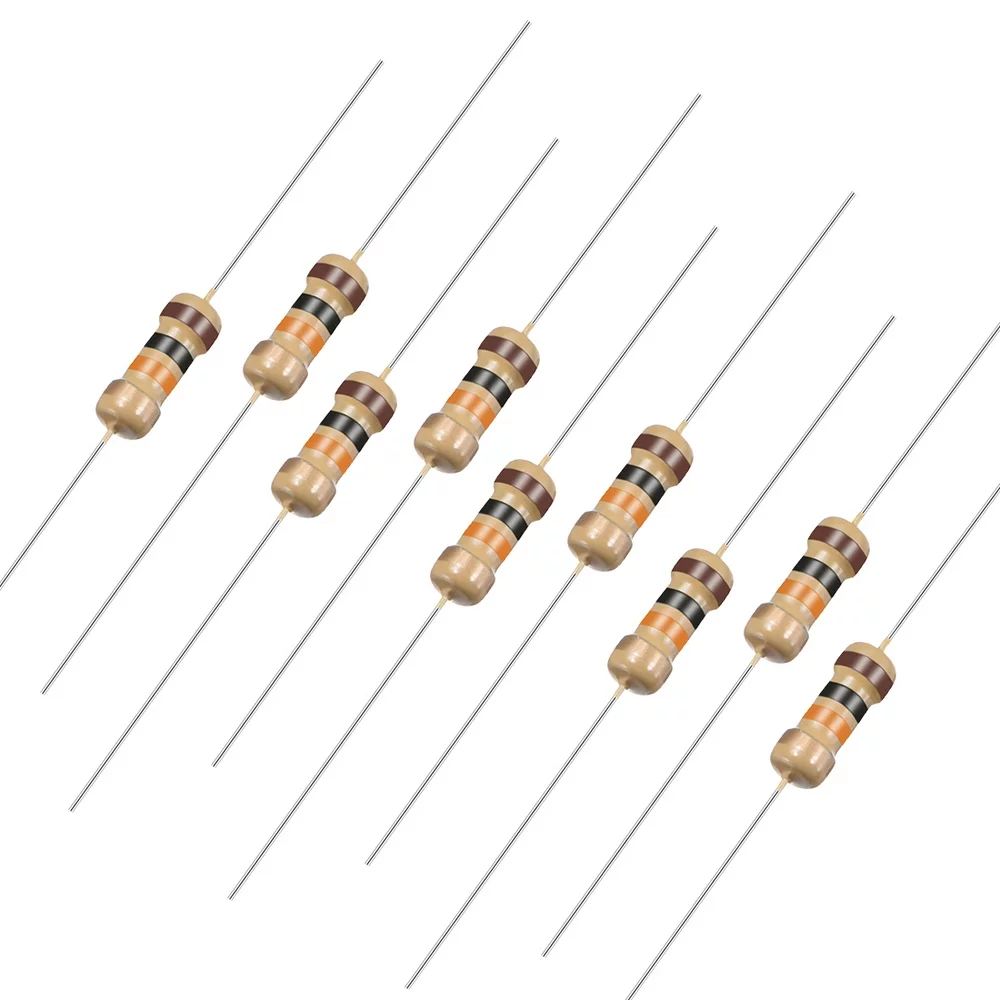
10 Ohm 0.25W Carbon Film Resistor (Pack of 50)
Build gain-setting resistor networks for your differential amplifier projects. Stock a range of resistor values for flexible circuit design.
Real-World Applications
Differential amplifiers appear in virtually every precision measurement system. Here are the most common applications relevant to Indian makers and engineers:
Wheatstone Bridge Sensors
Strain gauges, load cells, and pressure sensors are almost always configured as Wheatstone bridges. The bridge output is a small differential voltage (1–100 mV full scale) sitting on a large common-mode voltage (half the supply). An INA with a gain of 100–500× amplifies the signal while rejecting the common-mode, giving a full-scale output compatible with a microcontroller ADC.
Thermocouple Amplification
A thermocouple outputs approximately 40–60 µV/°C (type K). To cover a 0–500°C range (0–25 mV), a gain of 100–200× is needed. The thermocouple leads are differential (neither is grounded), making an INA the ideal interface. Cold-junction compensation is added separately.
ECG and Biomedical Signals
ECG (electrocardiogram) signals are 0.5–5 mV differential between two body electrodes, with 50 Hz common-mode interference of up to several volts from the body’s capacitive coupling to power lines. A high CMRR INA (>100 dB) is mandatory. This is the basis of all commercial ECG machines and heart rate monitors.
RS-422 and RS-485 Line Receivers
Industrial serial communication standards RS-422 and RS-485 use differential signalling. A differential line receiver (which is essentially a high-speed differential amplifier with a comparator threshold) receives the signal and rejects noise picked up along long cable runs. This is why RS-485 works reliably over 1200 metres in noisy factory environments while RS-232 fails at 15 metres.
Audio Balanced Inputs
Professional audio equipment uses balanced (XLR) connections with differential signalling. A differential amplifier at the input of each channel rejects noise induced in the cable, allowing long cable runs without hum pickup — essential in stage, studio, and broadcast setups.
Design Tips and Component Selection
- Use 1% or 0.1% metal film resistors: CMRR is directly limited by resistor matching. 5% carbon film resistors give poor CMRR. 1% metal film (MFR) resistors are the minimum for good results. 0.1% resistors or matched resistor networks give excellent CMRR.
- Decouple the op-amp supply: Place 100 nF ceramic capacitors from each supply pin to ground, directly at the IC pins. Add 10 µF electrolytic capacitors at the power entry point.
- Balance source impedances: For high CMRR, the impedance seen from each input to ground must be balanced. If V1 has a 100 Ω source impedance and V2 has 50 Ω, the mismatch creates a CMRR error. Use matched input protection resistors.
- Consider op-amp offset voltage: Op-amp input offset voltage (Vos) is amplified by the closed-loop gain. An LM358 has Vos up to 7 mV — at a gain of 100×, this becomes 700 mV output offset. For precision applications, use low-offset op-amps (OPA2134, LT1013, AD8221 with Vos < 50 µV).
- Watch for slew rate limits at high gain: High-gain amplifiers with wide bandwidth can slew-rate limit on fast transients. Ensure the op-amp’s slew rate (in V/µs) is sufficient for the maximum signal frequency and amplitude.
How to Build and Test the Circuit
Follow these steps to build and test a basic differential amplifier on a breadboard:
- Gather components: One LM358 or LM741 op-amp, four 10 kΩ resistors (for unity gain) or four resistors in ratio 1:10 (R1=R3=10kΩ, R2=R4=100kΩ for gain of 10), one 100 nF decoupling capacitor, dual supply (±12V or ±9V) or single supply with midpoint bias.
- Wire the circuit: V1 → R1 → inverting input (pin 2), feedback R2 from pin 6 to pin 2. V2 → R3 → non-inverting input (pin 3), R4 from pin 3 to ground. Power V+ to pin 8, V− to pin 4 (LM741). Place 100 nF from each supply pin to ground.
- Test differential mode: Set V1 = 1V, V2 = 2V. For gain 10×, expect Vout = 10 × (2−1) = 10V. If using ±12V supply, this is achievable without clipping.
- Test common mode: Set V1 = V2 = 2V. Ideally Vout = 0V. In practice, with 5% resistors, expect a few tens of millivolts of output — this is your common-mode error.
- Calculate CMRR: CMRR = 20 × log10(differential gain / common-mode gain). With gain = 10 and common-mode output = 20 mV for 2V common-mode input, Acm = 0.01, CMRR = 20 × log10(10/0.01) = 20 × log10(1000) ≈ 60 dB.
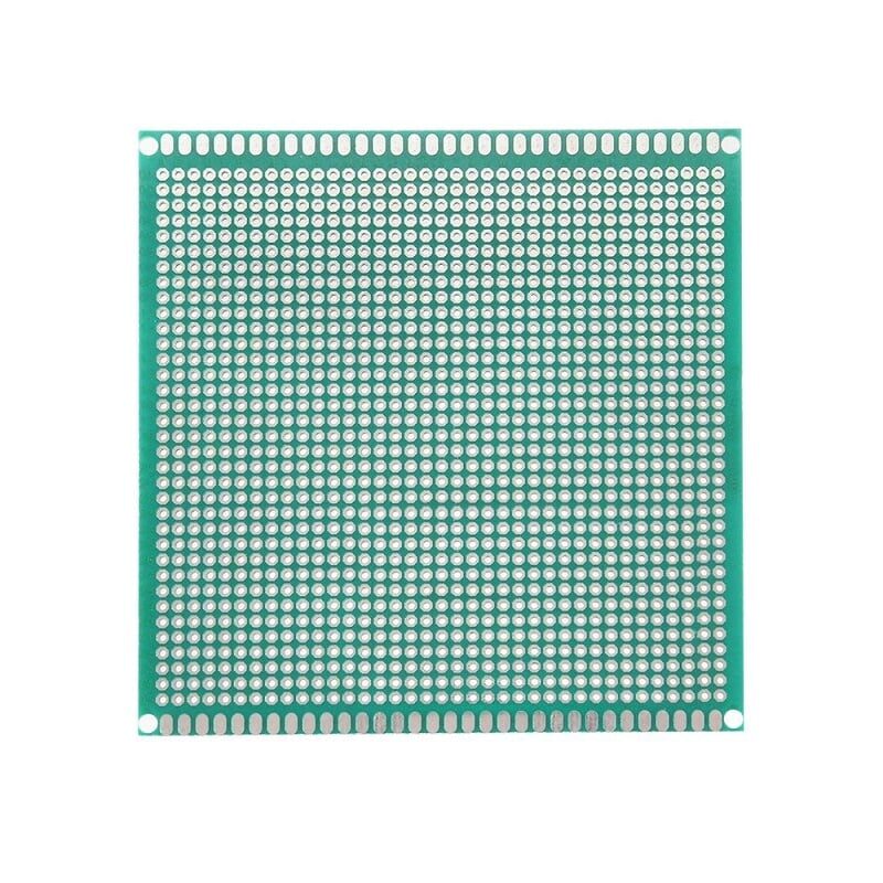
10×10 cm Universal PCB Prototype Board Single-Sided 2.54mm
Once you have verified your differential amplifier design on a breadboard, transfer it to a prototype PCB for a permanent, reliable circuit. The 10×10 cm size is ideal for op-amp signal conditioning boards.
Frequently Asked Questions
What is the difference between a differential amplifier and an instrumentation amplifier?
A differential amplifier (single op-amp design) has limited input impedance and moderate CMRR. An instrumentation amplifier (three op-amp design or integrated INA IC) adds high-impedance input buffers with gain, achieving very high CMRR and near-infinite input impedance. INAs are preferred for sensor interfaces; the single op-amp differential amplifier is suitable for general-purpose applications with low source impedance.
Why does CMRR decrease at higher frequencies?
Op-amp open-loop gain decreases with frequency. As gain falls, the ability to maintain balance between the inverting and non-inverting paths decreases, reducing CMRR. Additionally, stray capacitance creates slight phase differences between paths. This is why INA specifications include CMRR vs frequency curves — always check CMRR at the highest frequency component in your signal.
Can I use a differential amplifier with a single supply (e.g., 5V only)?
Yes, but with constraints. You need the output to swing above 0V — even if the differential input is zero. Add a virtual midpoint (2.5V) using a voltage divider or reference IC, connect it to the non-inverting input’s ground resistor (R4), and use a rail-to-rail op-amp. The output will swing around 2.5V, which you subtract in software after ADC conversion.
What value resistors should I use for a differential amplifier?
The ratio determines gain, but absolute values affect input impedance and noise. Higher resistance means lower thermal noise current (Johnson noise) but higher susceptibility to input bias current errors. For general-purpose work, 10 kΩ for R1/R3 and 10–100 kΩ for R2/R4 (gain 1–10×) is a good starting point. For low-noise designs, use 1–10 kΩ values. Always use 1% metal film resistors.
How do I choose the right op-amp for a differential amplifier?
Key parameters: sufficient GBP (gain × bandwidth product) for your application frequency; low input offset voltage Vos (critical for high-gain circuits); low input bias current Ib (critical for high source impedance); appropriate supply voltage range (single or dual, 3.3V or 5V or ±12V); package availability. For beginners, the LM358 (dual, single-supply, ₹5) covers most basic projects. For precision work, consider OPA2134 or AD8221.
From resistors and capacitors to prototyping boards and sensor modules, Zbotic has everything you need to build precision differential amplifier circuits. Fast shipping across India. Browse the Electronics Basics category and start your next analog project.


Add comment