
Boost Converter Basics: Inductor, Switch and Diode Operation
Understanding boost converter basics is one of the most valuable skills you can develop in electronics. A boost converter (also called a step-up converter) takes a lower input voltage and converts it to a higher output voltage at reduced current — efficiently and with minimal waste. Unlike a simple resistor divider or linear regulator that only wastes energy to produce a lower voltage, a boost converter performs actual energy transformation. Whether you’re running a 12 V LED strip from a 3.7 V Li-ion battery, charging a 5 V device from two AA batteries, or building a custom power supply module, the boost converter is the tool for the job.
The Core Operating Principle
A boost converter seems to violate common sense — how can a circuit output more voltage than it receives? The answer is that it trades current for voltage. Power (P = V × I) is conserved (minus small losses). If the output voltage doubles, the output current is halved. No energy is created; it’s transformed.
The boost converter achieves this using two states of operation that alternate thousands of times per second:
State 1 — Switch ON (Energy Store): The MOSFET switch connects the inductor directly between Vin and GND. Current flows through the inductor and ramps up linearly, storing energy as a magnetic field. The output capacitor supplies load current during this time.
State 2 — Switch OFF (Energy Release): The MOSFET opens. The inductor, trying to maintain current flow, generates a voltage spike that adds to Vin. This combined voltage (Vin + V_inductor) forward-biases the output diode and pushes charge into the output capacitor, raising the output voltage above Vin. Current through the inductor ramps back down as it delivers energy to the output.
The fundamental insight: the inductor is an energy storage element, and the boost converter exploits the inductor’s property of resisting changes in current to “push” energy to a higher voltage level.
The Inductor: Energy Storage Engine
The inductor is the most critical component in a boost converter. Its behaviour is governed by the fundamental equation:
V = L × (dI/dt) — Voltage across inductor equals inductance times rate of current change
This means:
- When switch is ON: V_L = Vin, so dI/dt = Vin/L. Current ramps up at rate Vin/L amps per second
- When switch is OFF: V_L = Vout − Vin (negative), so current ramps down at rate (Vout−Vin)/L
Choosing inductor value (L):
The inductor value determines the ripple current ΔIL. A larger inductor means less current ripple (smoother current, lower peak currents, better EMI), but is physically larger and more expensive. The formula for peak-to-peak inductor ripple current is:
ΔIL = (Vin × D) / (L × fsw)
Where D is duty cycle (0 to 1), f_sw is switching frequency. For a 5 V → 12 V converter at 100 kHz: D = 1 − 5/12 = 0.583. For L=22 µH: ΔIL = (5 × 0.583) / (22×10⁻⁶ × 100,000) = 1.33 A peak-to-peak ripple.
Saturation current rating: Choose an inductor whose saturation current is higher than the peak inductor current (average current + ΔIL/2). If the inductor saturates, inductance drops dramatically, causing large current spikes that can destroy the switching MOSFET.
DC resistance (DCR): The inductor’s winding resistance causes conduction losses (I² × DCR). Lower DCR = higher efficiency. For a 1 A boost converter, keep DCR below 100–200 mΩ.
The Switch (MOSFET): Controlling Energy Flow
The switch is what allows the boost converter to operate — it alternately connects and disconnects the inductor from GND at high frequency. In modern boost converters, this is always an N-channel MOSFET due to its low on-resistance (Rds_on) and fast switching characteristics.
Key MOSFET Parameters for Boost Converters
| Parameter | Why It Matters | Typical Value |
|---|---|---|
| Vgs(th) | Must be driven below gate threshold by controller | 1–4 V |
| Rds(on) | Determines conduction losses (I² × Rds) | 1–100 mΩ |
| Qg (gate charge) | Determines switching losses (f × Vg × Qg) | 5–50 nC |
| Vds (breakdown) | Must exceed Vout + switching transient | 20–100 V |
In boost converter ICs (like XL6009, MT3608, LM2577), the MOSFET is integrated inside the chip along with the PWM controller and feedback circuitry. External discrete MOSFETs are used only in high-power or custom designs.
The switching waveform at the MOSFET drain shows: voltage swings between near-zero (switch ON, V_ds ≈ I_L × Rds_on) and approximately Vout + switching transient (switch OFF, diode forward voltage drops the overshoot). The gate driver must ensure fast, clean transitions to minimise switching losses.
The Diode: Directing Current to the Output
The boost converter diode (often called the freewheeling or catch diode) has one job: allow current to flow from inductor to output when the switch is off, and block reverse current when the switch is on.
When the MOSFET turns off, the inductor voltage adds to Vin, making the diode anode more positive than the output capacitor cathode. The diode conducts and energy flows to the output. When the MOSFET turns on, the diode anode is pulled toward GND (through the inductor). The diode blocks reverse current, preventing the output capacitor from discharging back through the switch.
Choosing the Right Diode
Schottky diodes are strongly preferred for boost converter applications because:
- Low forward voltage drop (0.2–0.4 V vs 0.7 V for silicon) — directly improves output voltage and efficiency
- No reverse recovery charge — silicon diodes have a recovery time during which they briefly conduct in reverse; Schottky diodes don’t, eliminating a significant switching loss at high frequencies
- Efficiency improvement: at 1 A output, replacing a 1N4007 (0.7 V) with a 1N5819 Schottky (0.4 V) saves 300 mW of heat — about 3% efficiency improvement
Diode voltage rating: The diode must withstand the full output voltage in reverse. Use a diode rated for at least 1.5× Vout. For a 12 V output, use a 20 V or higher diode. For a 24 V output, use 40 V or higher.
Synchronous rectification: High-efficiency modern boost converters replace the diode with a second MOSFET (synchronous rectifier) that is turned on when the main switch turns off. This replaces the ~0.4 V diode drop with the much lower I×Rds_on drop of a MOSFET, pushing efficiency above 95%.
Duty Cycle and Voltage Conversion Ratio
The relationship between input voltage, output voltage, and duty cycle D (fraction of time the switch is ON) is the most fundamental equation of boost converter design:
Vout = Vin / (1 − D)
(ideal, in continuous conduction mode)
Rearranging for duty cycle: D = 1 − (Vin / Vout)
Examples:
- 3.7 V Li-ion → 5 V USB: D = 1 − 3.7/5 = 0.26 (26% duty cycle)
- 5 V → 12 V: D = 1 − 5/12 = 0.583 (58.3%)
- 12 V → 24 V: D = 1 − 12/24 = 0.5 (50%)
- 3.3 V → 48 V: D = 1 − 3.3/48 = 0.931 (93.1% — extreme ratio, difficult)
Note that as D approaches 1.0 (100%), ideal theory suggests infinite voltage multiplication, but real-world losses (MOSFET Rds, inductor DCR, diode Vf) limit practical conversion ratios. Above D = 0.85–0.90, efficiency drops rapidly. For very high step-up ratios (>10:1), cascaded boost stages or a flyback/SEPIC converter is preferable.
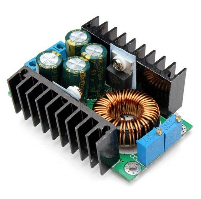
300W 10A DC-DC Step-Down Buck Converter Module
While a buck converter steps voltage down, understanding it alongside boost converters deepens your power electronics knowledge. This 300W adjustable module is great for high-current project testing.
Continuous vs Discontinuous Conduction Mode
Boost converters operate in two distinct modes depending on load current and inductor value:
Continuous Conduction Mode (CCM)
The inductor current never reaches zero between switching cycles. The current waveform is a continuous sawtooth riding above zero. CCM is the normal operating mode for heavy loads. Advantages: lower peak currents, lower EMI, simpler control. The voltage conversion formula V = Vin/(1-D) applies here.
Discontinuous Conduction Mode (DCM)
At light loads, the inductor current reaches zero before the next switching cycle begins. There’s a dead time where no current flows. DCM actually gives a higher output voltage than the CCM formula predicts for the same duty cycle. Advantages: faster transient response, simpler small-signal dynamics. Disadvantages: higher peak currents, more EMI.
Boundary Condition
The transition from CCM to DCM occurs at the critical inductance:
Lcrit = (Vout × D × (1−D)²) / (2 × fsw × Iout)
If L > L_crit at your load current, operation is CCM. If L < L_crit, it's DCM. Most practical designs target CCM at full load for predictable behaviour.
Practical Boost Converter Modules for Indian Projects
For most hobbyist projects, ready-made boost converter modules are far more practical than designing from scratch. Here are the most common options available in India:
MT3608 / XL6009 Boost Module
The most common ₹30–80 boost module on the market. Input: 2–24 V, output: adjustable up to 28 V, current up to 2–4 A. Uses an integrated switcher IC with external inductor, Schottky diode, and output capacitor. Adjustable output via a multi-turn pot. Good for 5 V USB output from Li-ion battery, LED driver circuits, and general voltage boosting.
150W AC-DC Buck Converter Module
For more demanding applications, a pre-built module that accepts AC input and produces regulated DC handles the boost/regulation internally. These are ideal for bench power supply builds.
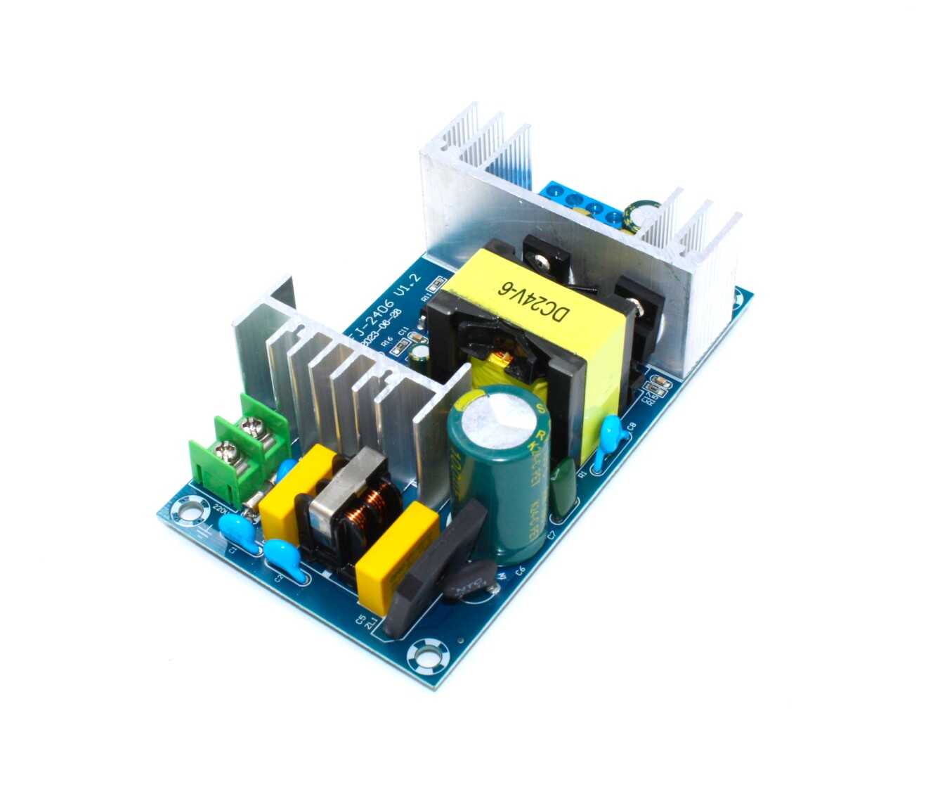
150W AC-DC Buck Converter 100V-240V to 24V
A reliable 24V supply module for powering boost converter experiments and high-power projects. Accepts Indian 230V AC mains input directly — plug and play.
Step-by-Step Design Example
Goal: 3.7 V Li-ion → 12 V @ 500 mA Boost Converter
Step 1: Calculate Duty Cycle
D = 1 − Vin/Vout = 1 − 3.7/12 = 0.692 (69.2%)
Step 2: Calculate Input Current
Assuming 85% efficiency: Pin = Pout/η = (12 × 0.5) / 0.85 = 7.06 W
Iin = Pin/Vin = 7.06/3.7 = 1.91 A average
Step 3: Select Inductor
Target ΔIL = 40% of Iin = 0.76 A peak-to-peak
At f_sw = 200 kHz: L = Vin × D / (ΔIL × f_sw) = 3.7 × 0.692 / (0.76 × 200,000) = 16.8 µH → use 22 µH
Peak current = 1.91 + 0.76/2 = 2.29 A → choose inductor rated for ≥3 A saturation current
Step 4: Choose Output Capacitor
For ΔVout = 50 mV ripple: C = Iout × D / (ΔVout × f_sw) = 0.5 × 0.692 / (0.05 × 200,000) = 34.6 µF → use 47 µF electrolytic + 100 nF ceramic in parallel
Step 5: Select Diode
Schottky diode, Vr ≥ 20 V, IF ≥ 1 A, low Vf: SS12 (1 A, 20 V) or SS24 (2 A, 40 V)
Step 6: Choose Controller IC
XL6009 (handles up to 4 A, 400 kHz, input 3–32 V, output up to 35 V) is an excellent match. Or design around LM2577-ADJ which can be configured for fixed or adjustable output.
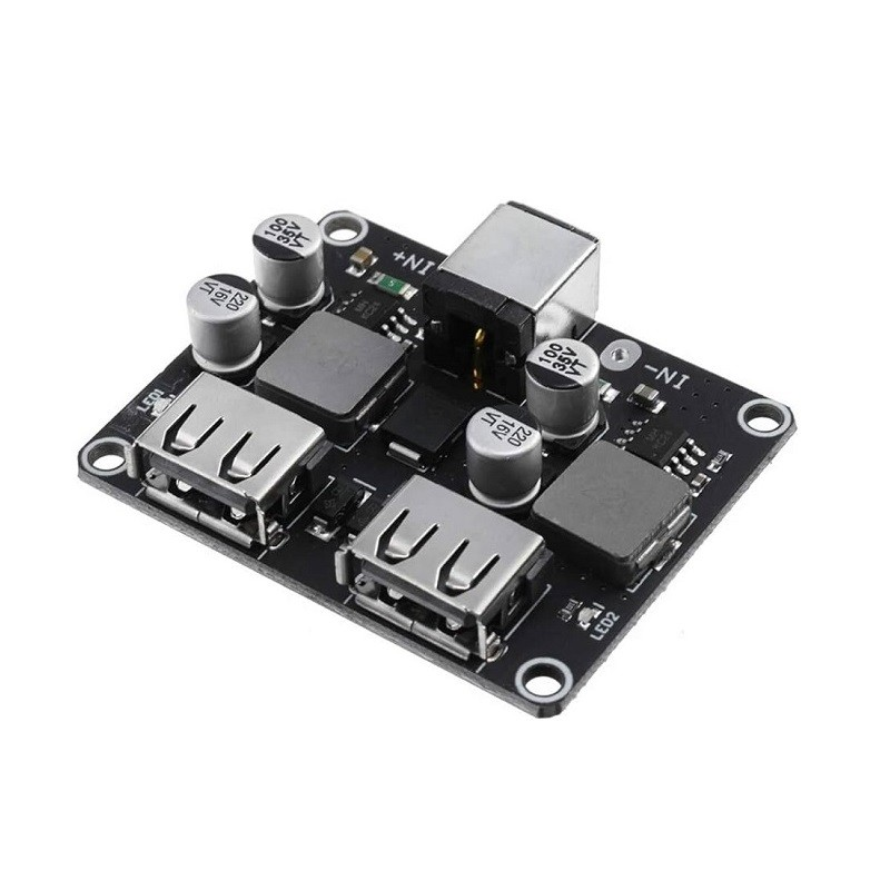
2-Channel USB QC3.0 DC-DC Buck Converter Module
This QC3.0 charging module demonstrates practical DC-DC conversion in action. Study its design to understand how commercial boost/buck converter circuits are engineered for real-world use.
Frequently Asked Questions
Q1: What is the maximum efficiency I can expect from a boost converter?
Well-designed boost converters using synchronous MOSFETs and careful layout can achieve 92–97% efficiency. Typical low-cost modules achieve 80–90%. The main losses are MOSFET switching losses, inductor DCR losses, diode forward drop, and controller quiescent current. Efficiency is typically highest at mid-load and drops at very light and very heavy loads.
Q2: Why does my boost converter oscillate or make a high-pitched whine?
The whine is from the inductor core vibrating at the switching frequency (audio range if f_sw < 20 kHz). Solution: increase switching frequency above 20 kHz. Oscillation usually indicates stability problems in the feedback loop — ensure adequate output capacitance, correct compensation (if external), and verify your duty cycle is within the controller's specifications.
Q3: Can a boost converter power itself from the output?
No — this would be a perpetual motion machine. A boost converter always requires an input voltage lower than the output voltage. You cannot bootstrap a boost converter from its own output.
Q4: What is the difference between a boost converter and a flyback converter?
Both step up voltage, but a flyback converter uses a transformer instead of an inductor, providing galvanic isolation between input and output. Flyback converters also easily produce multiple output voltages and can generate negative voltages. Boost converters are simpler, more efficient for lower power levels, but share a common ground between input and output.
Q5: How do I protect a boost converter from overload?
Most boost converter ICs include current limiting that folds back the output under overload. However, if the input current is not limited, the input source may be damaged. Add an input fuse sized for maximum expected input current. For the output, an electronic fuse circuit (using a MOSFET and comparator) can cut power faster than a traditional fuse — preventing damage in just a few microseconds.
Power Your Projects Efficiently
Boost converters are fundamental to modern electronics — from smartphones to electric vehicles. Understanding how the inductor, switch, and diode work together gives you the foundation to design any DC-DC converter topology. Explore Zbotic’s range of power supply modules and components to start your power electronics journey.


Add comment