
If you have ever powered up a switching circuit and watched your MOSFET or transistor fail in seconds, there is a good chance a voltage spike was the culprit. Snubber circuit design is one of the most underrated skills in power electronics, yet it is what separates a robust, long-lasting circuit from one that mysteriously destroys components. Whether you are building a motor driver, a SMPS, or an inductive load switcher, understanding how to suppress transient voltage spikes will save you components, money, and a lot of frustration.
What Is a Snubber Circuit?
A snubber circuit is a small network of passive components — typically a resistor and capacitor (RC), or a resistor, capacitor, and diode (RCD) — placed across a switching element or inductive load to absorb and dissipate the energy stored in parasitic inductance at the moment the switch opens. The name comes from the English word “to snub” meaning to cut short or suppress, which is exactly what these circuits do to dangerous voltage transients.
In the context of Indian electronics hobbyists and makers, snubbers are critically important when working with:
- Relay coil driver circuits (very common in Arduino/Raspberry Pi projects)
- MOSFET or IGBT based motor controllers
- Flyback and forward converter SMPS designs
- Solenoid and contactor switching circuits
- DC-DC buck and boost converter designs
Without a snubber, the voltage spike across the switching element can easily reach 5–10× the supply voltage, destroying MOSFETs, transistors, or driver ICs instantly.
Why Voltage Spikes Happen in Switching Circuits
Every real-world circuit has parasitic inductance — in PCB traces, wiring, and especially in inductive loads like motors, relays, and transformer windings. When a switch turns off and current through an inductance is suddenly interrupted, the inductor fights back. According to Lenz’s law, it generates a voltage spike to try to maintain that current: V = L × (dI/dt).
Consider a relay coil with just 10µH of inductance switching 500mA of current in 100ns (typical for a fast MOSFET). The resulting spike is:
V = 10×10⁻⁶ × (0.5 / 100×10⁻⁹) = 50V
If you are running a 12V circuit, that 50V spike will comfortably exceed the Vds breakdown of a low-cost MOSFET rated at 30V. Even with a 60V-rated device, repeated spikes degrade the oxide layer and eventually cause failure. This is why snubbers are not optional in production designs.
The spike’s energy is stored in the parasitic inductance: E = ½ × L × I². A snubber circuit provides a controlled path to dissipate this energy as heat in a resistor, rather than letting it appear as a destructive voltage spike.
Types of Snubber Circuits
There are four main snubber topologies you will encounter in practical electronics design:
1. RC Snubber (Boucherot Cell)
The most common and simplest snubber, consisting of a resistor and capacitor in series, placed across the switching element or load. The capacitor absorbs the spike energy during turn-off, and the resistor limits the discharge current during turn-on, preventing a new spike caused by the capacitor itself. RC snubbers are ideal for relay contacts, TRIAC circuits, and low-power switches.
2. RCD Snubber (Clamp Snubber)
A resistor, capacitor, and diode combination. The diode allows the capacitor to charge quickly during a spike but forces it to discharge slowly through the resistor. This is the go-to design for flyback converter primary switches and any circuit where the spike polarity is predictable. RCD snubbers are more efficient than RC snubbers because the capacitor only charges during turn-off events.
3. Diode Snubber (Freewheeling Diode)
Also called a flyback diode or suppressor diode, this is simply a diode placed across an inductive load (like a relay coil or motor) in reverse bias during normal operation. When the switch opens, the inductor’s spike forward-biases the diode, providing a circulating path for the current. This is the cheapest and most effective solution for relay drivers and DC motor circuits. The 1N4007 is the classic choice for low-speed switching.
4. TVS Diode Snubber
A transient voltage suppressor (TVS) diode clamps the voltage to a defined level. Unlike a freewheeling diode that provides a full current path, a TVS simply limits the peak voltage. TVS snubbers are excellent for protecting gate drivers and fast-switching GaN FET circuits where a freewheeling diode would be too slow.
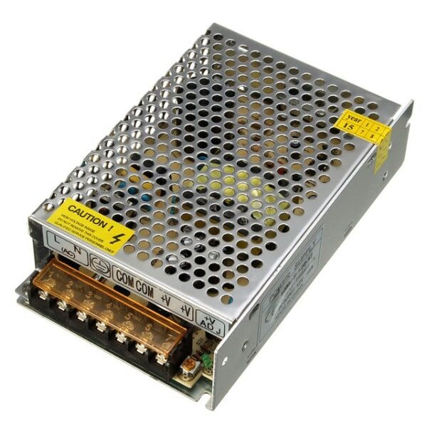
12V 10A SMPS – 120W DC Metal Power Supply
A reliable industrial-quality SMPS for bench testing your snubber circuit designs. The internal switching topology itself benefits from snubbers on its own switching FETs.
RC Snubber Design: Formulas and Calculations
Designing an RC snubber from first principles requires knowing the parasitic inductance of your circuit. This can be measured with an oscilloscope or estimated. Here is the systematic approach used by power electronics engineers:
Step 1: Measure the Ringing Frequency
Connect an oscilloscope across the switching element and capture the turn-off waveform. The damped oscillation frequency (f₀) tells you the resonant frequency of the parasitic LC circuit formed by the stray inductance (Ls) and switch capacitance (Cs).
Step 2: Estimate Parasitic Inductance
If you can estimate the stray capacitance (Cs, typically the MOSFET’s Coss or the PCB capacitance, usually 10–500pF), you can calculate Ls:
Ls = 1 / (4π² × f₀² × Cs)
Step 3: Calculate Snubber Component Values
The snubber capacitor (Cs_snub) should be 5–10× the parasitic capacitance. The snubber resistor (Rs) should be set to critically damp the circuit:
Rs = √(Ls / Cs_snub)
For a practical starting point on a 12V relay driver circuit with a typical 2N2222 or BC547 transistor switching a 12V/150mA relay coil, a 100Ω resistor and 10nF capacitor across the relay coil will work well in the vast majority of cases. If you are working with a 12V DC motor, start with 10Ω and 100nF.
Resistor Power Rating
Do not forget to size the snubber resistor correctly. The power dissipated in Rs is:
P_Rs = Cs_snub × Vdc² × f_sw
For a 12V circuit, 10nF snubber cap, switching at 1kHz: P = 10×10⁻⁹ × 144 × 1000 = 1.44mW. A standard ¼W resistor is more than adequate here.
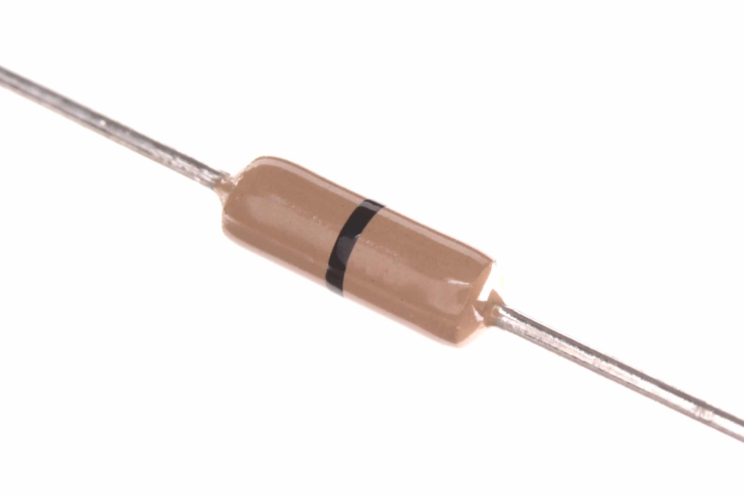
Carbon Film Resistors – 0.25W (Pack of 100)
Stock up on ¼W carbon film resistors for your snubber network experiments. Ideal for low-power switching circuits.
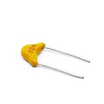
100nF Multilayer Ceramic Capacitor (Pack of 50)
100nF ceramic capacitors are the most commonly used value in RC snubber circuits for relay and motor switching applications.
RCD Snubber for Transformer-Based Circuits
When designing flyback converters or push-pull SMPS stages, the leakage inductance of the transformer creates massive voltage spikes on the primary MOSFET during turn-off. A simple freewheeling diode is not suitable here because there is no closed circuit for the current to flow through. This is where the RCD clamp snubber shines.
The RCD snubber works as follows: when the primary MOSFET turns off, the leakage inductance drives the drain voltage up. Once it rises above the DC bus voltage (Vbus + Vdiode), the clamp diode turns on and charges the snubber capacitor. The resistor then bleeds the energy from the capacitor between switching cycles, limiting the clamp voltage.
Design Equations for RCD Snubber
The clamp voltage (Vclamp) you want to set typically needs to be at least 1.3× the reflected output voltage (Vref) plus the DC bus:
- Choose Vclamp = Vbus + 1.5 × Vref (safe starting point)
- Rs = (Vclamp² × (1 – D)) / (Llk × Ipk² × f_sw) where D = duty cycle, Llk = leakage inductance, Ipk = peak current
- Cs = 5 / (Rs × f_sw) ensures adequate filtering
Use a fast recovery diode (like UF4007 or BYV26) for the clamp diode, not a 1N4007, as the slow recovery of the 1N4007 will cause it to conduct during part of the ON cycle and reduce efficiency.
Placement Tips and PCB Layout Considerations
Even a perfectly designed snubber can fail to work if it is placed poorly on the PCB. Here are the golden rules of snubber placement:
- Place snubbers as close as possible to the source of the spike. If you are snubbing a relay coil, put the RC directly across the coil terminals, not at the driver transistor. If snubbing a MOSFET’s drain-source, place the components directly adjacent to the device pads.
- Minimize trace inductance in the snubber loop. Keep the loop area formed by the snubber components as small as possible. Use wide, short traces. Every nH of inductance in the snubber loop reduces its effectiveness at high frequencies.
- Use appropriate capacitor types. For high-frequency snubbers (above 100kHz), use multilayer ceramic capacitors (MLCC) with low ESL. Electrolytic and tantalum caps have too high ESL at these frequencies. For AC mains snubbers, use X2-rated film capacitors only.
- Ground the snubber correctly. A snubber connected to a high-impedance ground or a ground with a long trace back to the actual power ground is less effective. Star ground the snubber return.
- Prototype on a proper PCB, not on a breadboard. Breadboard contact resistance and stray capacitance make measuring snubber effectiveness nearly impossible. Use a proper universal PCB for any serious snubber characterisation work.
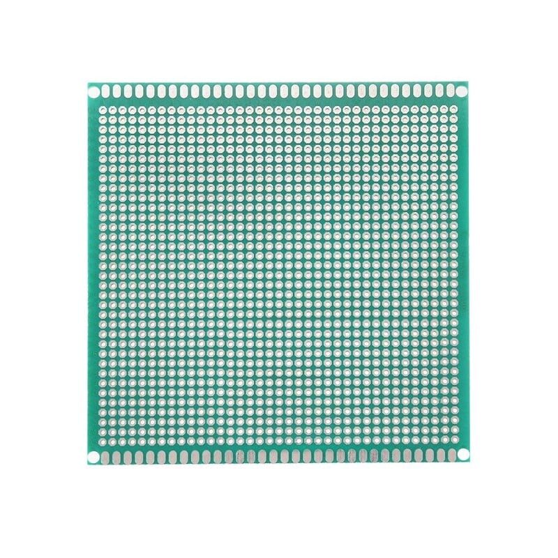
10×10 cm Universal PCB Prototype Board – Single Sided
Prototype your snubber and protection circuits on this standard 10×10cm single-sided perfboard before committing to a custom PCB layout.
Measuring Voltage Spikes with an Oscilloscope
You cannot design a snubber without first measuring the problem. An oscilloscope is an essential tool here. Here is the workflow to quantify spikes in your switching circuit:
- Connect a 10× probe across the switch (Drain-Source for a MOSFET, Collector-Emitter for a transistor). Never use a 1× probe for switching circuits — the probe cable capacitance will distort the measurement.
- Set the timebase to 100ns/div or faster. Voltage spikes from fast switching last only tens to hundreds of nanoseconds.
- Set the trigger to a rising edge on the switch voltage, at a level just above the DC bus voltage. This will capture the spike right after turn-off.
- Measure the peak voltage and the ringing frequency. If the peak exceeds the component’s rated Vds or Vce, a snubber is mandatory.
- After adding the snubber, re-measure to confirm the peak is suppressed and the ringing is damped. A good snubber will reduce ringing to less than 20% overshoot above the DC bus voltage.
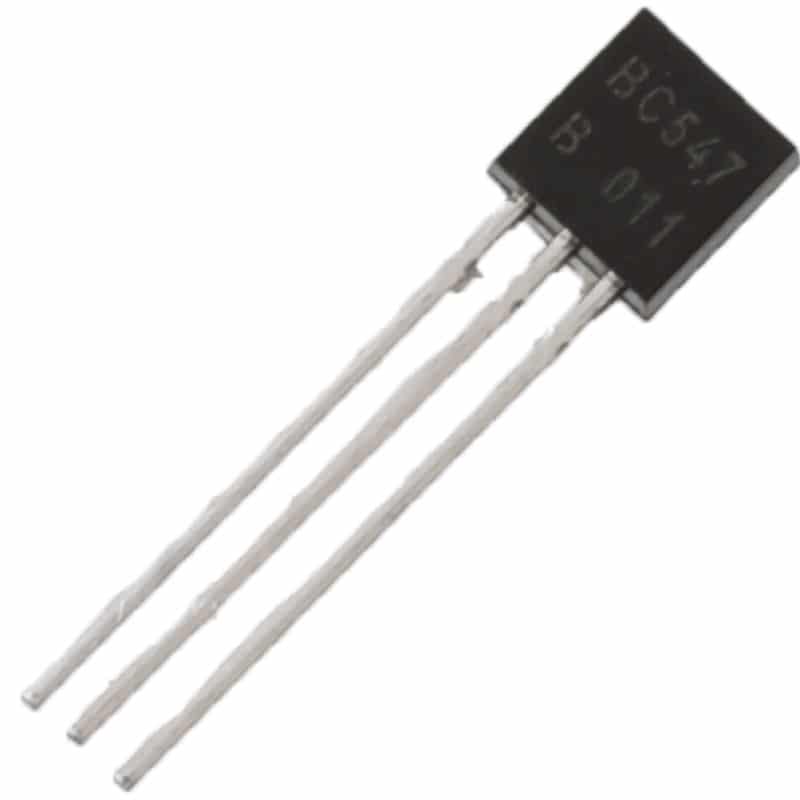
BC547 NPN Transistor TO-92 (Pack of 10)
The BC547 is a classic general-purpose transistor used in relay driver circuits — a prime application where snubbers prevent destruction from inductive kickback.
Frequently Asked Questions
Can I use any capacitor for an RC snubber?
No. For DC switching circuits (relay drivers, motor controllers), a standard multilayer ceramic capacitor (MLCC) with the appropriate voltage rating works well. For AC mains applications (TRIAC dimmers, relay contacts on mains voltage), you must use an X2-rated film capacitor rated for mains voltage. Using a standard MLCC on mains voltage is extremely dangerous.
Is a freewheeling diode the same as a snubber diode?
A freewheeling diode (also called a flyback diode or catch diode) is a specific type of snubber diode placed across an inductive DC load. All freewheeling diodes are snubbers, but not all snubbers are freewheeling diodes. A TVS diode used for spike clamping is also a snubber diode, but it does not provide a freewheeling path for current.
My relay keeps welding its contacts shut. Can a snubber fix this?
Contact welding is usually caused by excessive contact bounce and inrush current, not by inductive spikes. A snubber across the coil protects the driver transistor; a snubber across the contact (load side) protects the contacts themselves. A 0.1µF/100Ω RC snubber across the contacts will reduce arcing and extend contact life significantly for AC loads.
What values should I start with for a quick experiment?
For a 5–12V relay driver with a BC547 or 2N2222 transistor, a 1N4007 freewheeling diode across the relay coil is the simplest and most effective solution at zero cost complexity. For a MOSFET-based DC motor driver at 12V, try 100Ω + 10nF in series across the MOSFET Drain-Source as a starting point and adjust based on oscilloscope measurements.
Do I always need a snubber with fast MOSFETs?
Not always, but you should always check. Fast MOSFETs (switching in under 10ns) can generate significant spikes even from short PCB trace inductance. GaN FETs in particular are notorious for ringing. Check your circuit with an oscilloscope before deciding. If the peak voltage stays below 80% of the device’s Vds rating, you may not need a snubber.
Build Better, More Reliable Circuits
Browse Zbotic’s full range of passive components, transistors, and capacitors to build your own snubber and protection circuits. From ceramic capacitors to carbon film resistors, we have everything Indian makers need at great prices.


Add comment