
SEPIC Converter Explained: Flexible Input-Output Topology
When engineers need a DC-DC converter that can step voltage up or down while keeping the output polarity the same as the input — without the complexity of a 4-switch buck-boost — the SEPIC converter (Single-Ended Primary Inductance Converter) is often the answer. In this SEPIC converter explained guide, we’ll walk through the topology, working principle, design equations, and practical applications that make this architecture a favourite in battery management, LED lighting, and IoT power rails across India’s maker community.
What Is a SEPIC Converter?
SEPIC stands for Single-Ended Primary Inductance Converter. It is a switching power supply topology invented to address a specific gap in power electronics: the need for a non-inverting buck-boost converter with a simple single-switch architecture.
Here’s what makes the SEPIC unique:
- Non-inverting output: Output voltage polarity is the same as input voltage (positive in → positive out)
- Buck-boost capability: Output can be set above or below input voltage
- Single switch: Uses only one MOSFET (simpler gate driving than 4-switch buck-boost)
- Input current continuity: Input current is smooth and continuous — ideal for battery-powered systems sensitive to current spikes
It achieves this through a clever combination of two inductors and a series coupling capacitor. The trade-off is slightly higher component count compared to a pure buck or boost, and somewhat lower efficiency compared to a 4-switch synchronous buck-boost, but the single-switch simplicity makes SEPIC attractive for cost-sensitive designs.
The SEPIC Topology Explained
A SEPIC converter has the following key components arranged in a specific way:
- L1 (Input Inductor): Connected between the input voltage and the MOSFET drain. This is the “primary” inductance referred to in the name.
- Q1 (MOSFET Switch): The single switching element, controlled by a PWM signal from the controller IC.
- Ccoupling (Series Capacitor): The energy transfer capacitor between the two inductor stages. This is what differentiates SEPIC from a simple boost converter. It blocks DC while coupling AC energy.
- L2 (Secondary Inductor): Connected between the coupling capacitor and the output. L1 and L2 are often wound on the same core (coupled inductors) to save space, though they can also be separate inductors.
- D1 (Output Diode): Freewheeling diode that conducts when the MOSFET is off, delivering energy to the output. A Schottky diode is preferred for lower forward voltage drop.
- Cout (Output Capacitor): Filters the output voltage ripple.
The coupling capacitor Ccoupling typically charges to the input voltage Vin in steady-state operation. This DC voltage across the capacitor is what allows the topology to produce output voltages both above and below the input.
How a SEPIC Converter Works — Step by Step
The SEPIC converter has two distinct phases of operation per switching cycle:
Phase 1: MOSFET ON (Energy Storage)
When Q1 turns on:
- Current through L1 ramps up, storing energy from the input source
- The coupling capacitor Ccoupling (charged to ≈ Vin) provides energy to L2, ramping up its current
- The output diode D1 is reverse-biased — no current flows to the output
- The output capacitor Cout supplies the load current during this phase
Phase 2: MOSFET OFF (Energy Delivery)
When Q1 turns off:
- L1’s collapsing magnetic field drives current through the output diode D1 to the output
- L2’s collapsing field also drives current through D1 to the output
- Both inductors now series-add their voltages to charge Cout and supply the load
- The coupling capacitor Ccoupling recharges from L1’s energy
The output voltage is determined by the duty cycle: Vout = Vin × D / (1 – D), where D is the duty cycle of Q1. This is the same relationship as a boost converter — but the SEPIC achieves it with non-inverting polarity through the coupling capacitor.
Key Insight: Why Non-Inverting?
In a traditional inverting buck-boost, the inductor flips voltage polarity because one end is referenced to ground. In SEPIC, the coupling capacitor effectively provides a floating reference for L2, so both L1 and L2 current contributions add constructively at the output node in the same polarity as the input.
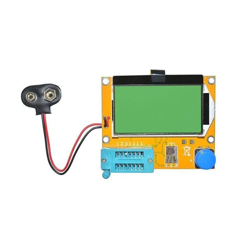
LCR-T4 Transistor Tester — Resistance, Capacitance & ESR Meter
Essential for verifying inductors, capacitors, and MOSFETs used in your SEPIC converter design. Measures ESR, capacitance, and component type automatically.
Design Equations and Component Selection
Let’s walk through sizing each component for a practical SEPIC design example: Input: 2.7V–5.5V, Output: 3.3V at 500mA (a common IoT supply from a Li-Ion cell).
Step 1: Determine Duty Cycle Range
Using D = Vout / (Vin + Vout):
- At Vin = 2.7V: D = 3.3 / (2.7 + 3.3) = 0.55 (55%)
- At Vin = 5.5V: D = 3.3 / (5.5 + 3.3) = 0.375 (37.5%)
Controller ICs need to handle 37.5–55% duty cycle range — easily achieved by most switching regulators.
Step 2: Inductor Selection
For coupled inductors (L1 = L2 = L), the inductance is:
L = Vin_min × D_max / (f × ΔIL)
Choose 20–30% ripple current (ΔIL = 0.3 × Iout). At 500mA output, ΔIL ≈ 150mA. At 500 kHz switching frequency:
L = 2.7 × 0.55 / (500,000 × 0.15) ≈ 19.8 µH → use 22 µH
Saturation current rating should be at least 1.5× peak inductor current: ~1.5 × (500mA + 75mA) ≈ 860mA. Choose a 22 µH coupled inductor rated 1A or more.
Step 3: Coupling Capacitor Selection
The coupling capacitor Ccoupling must handle the full input voltage with sufficient ripple current capacity. Minimum capacitance:
Ccoupling = D_max × Iout / (f × ΔVcoupling)
With ΔVcoupling = 5% of Vin_min = 0.135V:
Ccoupling = 0.55 × 0.5 / (500,000 × 0.135) ≈ 4.07 µF → use 4.7 µF, 10V-rated ceramic capacitor
Step 4: Output Capacitor Selection
For 1% output ripple (33mV on 3.3V):
Cout = Iout × D_max / (f × ΔVout) = 0.5 × 0.55 / (500,000 × 0.033) ≈ 16.7 µF → use 22 µF, 10V ceramic
Step 5: MOSFET Selection
The MOSFET in a SEPIC sees a voltage stress of Vin + Vout (worst case). For our example: 5.5 + 3.3 = 8.8V → use a MOSFET with at least 20V Vds rating. Peak current through the MOSFET equals the sum of peak inductor currents in both L1 and L2.
Recommended Controller ICs for SEPIC
- LM5022 (TI): High-voltage SEPIC/Boost controller, 6–75V input, excellent for automotive
- MAX1771: Low-voltage SEPIC, popular for battery-powered IoT devices
- LT1308: Very low quiescent current, ideal for low-power applications
- MC34063A: Classic, widely available in India, budget-friendly for low-power SEPIC designs
0.1/100nF TH Multilayer Ceramic Capacitor (Pack of 50)
High-quality bypass and decoupling capacitors. Use in series with bulk capacitors for best EMI suppression in your converter design.
Advantages and Limitations
Advantages of SEPIC Converter
- Non-inverting output: Same polarity as input — no level-shifting needed at the output
- Single switch: One MOSFET = one gate driver = simpler PCB and controller
- Continuous input current: L1 ensures smooth input current draw — very battery-friendly, reduces input EMI
- Buck-boost range: Works from below to above input voltage seamlessly
- Input-to-output isolation capability: The coupling capacitor provides AC isolation; no direct DC path between input and output. This is a safety advantage in some applications.
- Scalable: Works from milliwatts (IoT sensors) to tens of watts (LED drivers) by scaling component sizes
Limitations of SEPIC Converter
- Discontinuous output current: Unlike the input, the output current is pulsed. Higher output capacitance is required to manage output ripple.
- More components than pure buck/boost: Two inductors + coupling capacitor add cost and PCB area
- Lower efficiency than 4-switch synchronous buck-boost: The output diode (non-synchronous) causes a forward voltage drop loss. Replacing with a synchronous switch is complex.
- Higher switch voltage stress: MOSFET sees Vin + Vout, requiring a higher-rated (and typically costlier) device
- Complex dynamics: Right-half-plane (RHP) zero in the transfer function makes compensation loop design tricky at wide duty cycle ranges
Common Applications for SEPIC Converters
1. Single-Cell Li-Ion Battery Systems
A single Li-Ion cell discharges from 4.2V to 3.0V. If your system needs 3.3V (for microcontrollers) or 3.7V (for some RF modules), a SEPIC converter operates across the full battery range without dropout. This eliminates the need for LDO linear regulators that waste energy as heat when the battery is full.
2. LED Drivers
LEDs require constant current drive. SEPIC topology is excellent here because it handles wide input voltage ranges (e.g., a 3-cell NiMH pack from 3.6V to 4.5V) while maintaining constant LED current. Many dedicated LED driver ICs use SEPIC or SEPIC-like topologies internally.
3. USB Power Delivery from Variable Sources
Generating a stable 5V from sources like wind turbines, solar panels, or multi-cell battery packs that may be above or below 5V — the SEPIC handles all cases with a single stage.
4. Automotive 12V Rail Regulation
Car battery voltage swings from 9V (cold crank) to 14.4V (alternator), with possible load dump spikes to 40V. A SEPIC with an appropriately rated MOSFET can ride through the entire automotive voltage range and deliver a stable 12V or 13.8V for sensitive electronics.
5. IoT Sensor Nodes
Low-power sensor nodes often run from coin cells or small LiPo cells. A SEPIC with a low-quiescent-current controller (like the LTC3105 for energy harvesting) can efficiently boost or buck the cell voltage to power a microcontroller and radio module.
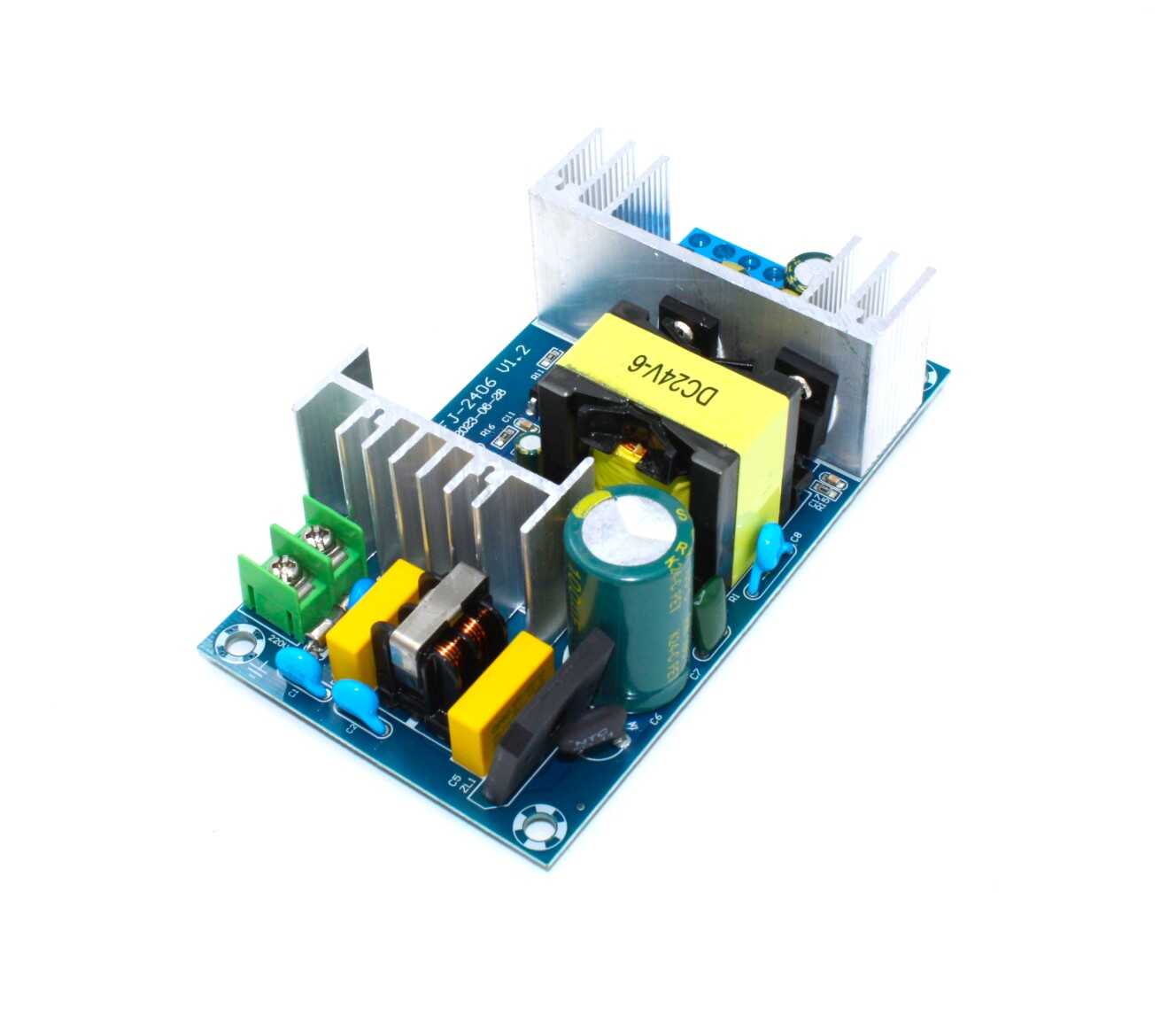
150W AC-DC Buck Converter 100V-240V to 24V 6A-9A
Use as a bench power source for testing your SEPIC converter prototypes. Provides a stable, high-power 24V DC input for experiments.
SEPIC vs Buck-Boost vs Ćuk
| Feature | SEPIC | Inverting Buck-Boost | Ćuk |
|---|---|---|---|
| Output Polarity | +ve (same as input) | -ve (inverted) | -ve (inverted) |
| Input Current | Continuous | Pulsed | Continuous |
| Output Current | Pulsed | Pulsed | Continuous |
| Number of Switches | 1 MOSFET + 1 diode | 1 MOSFET + 1 diode | 1 MOSFET + 1 diode |
| Ripple | Low input, higher output | High input and output | Very low both sides |
| Common Use | Battery power, LED drivers | Negative supply generation | Noise-sensitive circuits |
Frequently Asked Questions
Q1: Why is the coupling capacitor in SEPIC important?
The coupling capacitor (Ccoupling) is the key element that makes SEPIC non-inverting. It stores energy and provides a floating voltage reference between the two inductor stages. In steady state, it charges to approximately Vin. Without it, the topology would simply be a boost converter (if only L1 is considered) with no buck capability.
Q2: Can I use separate inductors instead of coupled inductors in a SEPIC?
Yes, you can use two separate inductors. The circuit still functions correctly. However, coupled inductors (wound on the same core) offer advantages: they cancel AC flux in the core (reducing core losses), reduce EMI, save PCB area, and can reduce ripple. The value of L1 and L2 must be equal when using separate inductors, but coupling ratio can be adjusted when using a single coupled inductor core.
Q3: What is the biggest design challenge with SEPIC converters?
The biggest challenge is the right-half-plane (RHP) zero in the transfer function. This zero limits the bandwidth of the control loop — if your feedback loop tries to respond too quickly, the converter goes unstable. The fix is to design a slow, well-compensated feedback loop with sufficient phase margin (at least 45°), and use a Type-II or Type-III compensator in the error amplifier.
Q4: How do I choose between SEPIC and a 4-switch synchronous buck-boost?
Use SEPIC when: cost is a priority, output power is under 20W, efficiency can be 88–91%, and single-switch gate drive simplicity matters. Use a 4-switch synchronous buck-boost when: efficiency above 93% is needed, output power exceeds 20–30W, thermal performance is critical, and you can afford the more complex gate driver IC and PCB layout.
Q5: Does the SEPIC converter produce significant EMI?
All switching converters produce EMI. SEPIC produces continuous input current (good for input EMI) but pulsed output current (higher output ripple and EMI). To manage EMI: use shielded coupled inductors, add an input EMI filter (small LC filter before the converter input), keep switching node traces short and away from sensitive signals, and use spread-spectrum frequency modulation in the controller if available.
Explore Power Electronics Components at Zbotic
Building a SEPIC or other switching converter? Zbotic stocks capacitors, resistors, transistors, and prototyping boards for all your power electronics projects. Fast shipping across India.


Add comment