
Reflow Soldering with Hot Plate: DIY SMD Assembly Guide
Reflow soldering with a hot plate is the most accessible and cost-effective way to assemble SMD boards at home. Unlike a dedicated reflow oven (which costs ₹8,000 and up), a basic electric hot plate or a repurposed cooking plate costs under ₹500 and can solder an entire PCB in under 5 minutes once you understand the technique. This guide walks you through the complete DIY SMD assembly workflow — from applying solder paste and placing components to executing the reflow cycle and inspecting results. Whether you’re building your first custom PCB or scaling up from hand-soldering, this guide will level up your workshop.
How Reflow Soldering Works
Reflow soldering uses heat — not a soldering iron — to melt solder paste that has been pre-applied to PCB pads. Components are placed on the wet paste (which is sticky), then the entire board is heated in a controlled temperature profile. At the peak temperature, the solder spheres in the paste melt and fuse to both the component termination and the PCB pad, creating solid, reliable joints simultaneously across the whole board.
The key advantages over hand-soldering every pad:
- All joints made at once: A board with 200 pads is reflowed in one 5-minute cycle vs. 200 individual iron touches.
- Self-alignment: Surface tension in molten solder physically pulls small components into alignment on their pads — boards often look cleaner than hand-soldered ones.
- Consistent joint quality: No cold joints from rushing, no heat damage from prolonged iron contact.
- Access to small packages: QFN and 0402 components that are nearly impossible to hand-solder are straightforward with reflow.
Hot Plate Options for DIY Reflow
You have several options for the heat source, each with trade-offs:
1. Dedicated SMD Hot Plate / Preheater
Purpose-built PCB preheater plates with PID temperature control and a flat aluminium surface. These cost ₹1,500–₹5,000 and are the cleanest solution — even heating, accurate temperature display, and programmable profiles. They’re designed specifically for this task.
2. Cheap Electric Stove / Induction Cooktop
A single-burner electric stove (coil or cast-iron plate, not induction) can be used. The challenge is that these have poor temperature control — they reach temperatures of 250–450°C at full power, which is too high. Use on the lowest setting and monitor with an IR thermometer or thermocouple. Induction cooktops don’t work (PCBs are not magnetic).
3. Skillet / Frying Pan on Gas
Possible in a pinch. Heat the skillet on very low flame, place the PCB, and monitor temperature constantly with an IR gun. Not recommended for production but functional for occasional one-off boards. Risk of localised hot spots and difficulty controlling ramp rate.
4. Modified Toaster Oven
Technically a reflow oven, not a hot plate, but popular in India for larger boards. Modify a ₹1,500 toaster oven by adding a thermocouple and relay controller. DIY cost: ₹2,000–₹3,000 total. Provides better temperature uniformity for larger boards and allows proper profiling.
Recommendation for beginners: A cheap single-burner electric hot plate on low setting with an IR thermometer (or K-type thermocouple) gives you the fastest path to soldering your first SMD board without a large investment.
Choosing and Applying Solder Paste
Solder paste is the critical consumable. Key specifications:
Alloy Composition
- Sn63Pb37 (Leaded, 63/37): Melts at 183°C. Easier to work with, more forgiving, excellent joint quality. Not RoHS compliant but fine for hobbyist use.
- SAC305 (Lead-free, Sn96.5/Ag3/Cu0.5): Melts at 217–220°C. Requires higher peak temperatures (245–250°C). Produces shinier joints. Required for commercial products.
Paste Type
- No-clean flux: Most common. Flux residue is non-corrosive and can be left on the board. Ideal for most projects.
- Water-soluble flux: More active (better wetting), but residue MUST be washed off with deionised water within hours or it corrodes tracks.
- Rosin-based: Traditional, very reliable. Clean with isopropyl alcohol if desired.
Storage and Shelf Life
Solder paste must be refrigerated (4–10°C) when not in use. Bring to room temperature (about 30 minutes) before opening — condensation inside the jar will ruin the paste. Shelf life is typically 6 months refrigerated. Dry or separated paste produces poor joints — discard it.
Application by Syringe
For small quantities or rework, apply paste directly from a syringe. The goal is to cover each pad completely but not overflow onto the solder mask between pads. Use a stencil for consistent results on full boards.

1.2M AC 10A 250V Power Supply Adapter Cord Cable EU Plug
A robust 10A 250V AC power cord for powering your hot plate, reflow station, or soldering equipment. 1.2m length gives comfortable reach from the bench to wall socket.
Using Stencils for Perfect Paste Application
A solder paste stencil is a thin stainless steel or mylar sheet with laser-cut openings matching your PCB’s pad layout. It’s the fastest and most consistent way to apply paste to a full board.
How to Use a Stencil
- Align the stencil over the PCB using registration marks or simply by eye-aligning the cutouts with the pads. Tape the corners to hold position.
- Apply paste: Drop a line of paste across one end of the stencil. Use a squeegee (an old credit card works) to drag the paste across the stencil in one smooth pass at 45°.
- Lift the stencil: Lift straight up slowly. The paste should be deposited on every pad in neat, raised squares.
- Inspect: Check for missing pads, smears, or bridged paste. Touch up with a syringe if needed.
Stencils can be ordered with your PCB from JLCPCB, PCBWay, or locally in India from PCB manufacturers for ₹300–₹800 depending on board size. For prototype runs, a mylar stencil cut by a Cricut or laser cutter works for 0805 and larger.
Component Placement Tips
After paste application, you have a working window before the paste dries out (typically 4–8 hours at room temperature, less in Indian summer heat). Place all components before reflowing.
- Use tweezers or vacuum pickup: Fine tweezers for most components; a vacuum pencil (bulb-type or electric) speeds up placement significantly.
- Polarised components first: ICs, diodes, polarised capacitors. Mark pin 1 on the PCB silkscreen and confirm orientation carefully.
- Passive components last: Resistors and non-polarised capacitors — these are easier to place and don’t need orientation.
- Light press: Gently press each component down into the paste so it contacts the pads, not just sitting on top of the paste ball.
- Reel tape trick: Cut the component tape, peel back the cover tape slowly, and use tweezers to pick directly from the tape carrier — much faster than picking from a loose component tray.

0.1/100nF – TH-Multilayer Ceramic Capacitor (Pack of 50)
Through-hole 100nF MLCC bypass capacitors for mixed SMD/TH boards. Place these on IC power supply pins during prototyping while your SMD boards use their surface-mount equivalents.
The Reflow Process Step by Step
Setup
- Place the hot plate on a stable, heat-proof surface. Keep a fire extinguisher or CO2 nearby (good lab practice).
- Have an IR thermometer or thermocouple ready to monitor plate surface temperature.
- Have tweezers ready for component retrieval if something shifts during reflow.
The Reflow Cycle
- Preheat (room temp → 150°C): Turn the hot plate to its lowest-medium setting. Place the loaded PCB on the plate. The board should heat slowly — 1–3°C per second is ideal. This is the preheat phase: flux activates and volatiles escape without spattering paste.
- Soak (150°C → 180°C for leaded / 150–200°C for lead-free): Hold at this range for 60–90 seconds. This equalises temperature across the board and completes flux activation. You’ll see the paste begin to change texture.
- Reflow / peak (183°C+ for leaded / 217°C+ for lead-free): Increase heat slightly. The paste melts — you’ll see a distinct change as the grey paste becomes shiny silver liquid solder. All joints reflow simultaneously. Hold at peak (typically 200–210°C for leaded, 235–250°C for lead-free) for 20–30 seconds.
- Cooling: Slide the board off the plate or turn off heat. Let cool at room temperature. Don’t blow on it or cool rapidly — thermal shock can crack ceramic capacitors. Inspect once cool to touch.
Temperature Profiles Explained
The standard reflow profile for leaded solder paste (Sn63Pb37):
| Phase | Temperature Range | Duration | Purpose |
|---|---|---|---|
| Preheat | 25°C → 150°C | 60–90s | Evaporate solvents, begin flux activation |
| Soak | 150°C → 180°C | 60–120s | Equalise temp, complete flux activation |
| Reflow | 183°C → 210°C peak | 30–60s above liquidus | Solder melts, joints form |
| Cooling | 210°C → room temp | 1–3°C/s | Solder solidifies; avoid rapid cooling |
Why does the profile matter? Ramp too fast → paste splatters → solder balls everywhere. Soak too short → cold joints and poor wetting. Peak too high or too long → component damage and board delamination. Too rapid a cool → thermally shocked capacitors. For a cheap hot plate, you’re approximating this profile by adjusting power level and timing — practice on a blank PCB first.

BAKON Soldering Iron Tip 900M-T-I
After hot plate reflow, you’ll need to touch up skewed components or rework individual joints. This precision I-type soldering tip is ideal for post-reflow rework on fine-pitch SMD pads.
Post-Reflow Inspection and Rework
After the board cools, inspect under magnification before powering it up:
What Good Joints Look Like
- Leaded joints: bright silver, concave fillets, smooth surface
- Lead-free joints: slightly duller, more granular appearance is normal — still shiny but not mirror-bright
- All component terminations should be wetted (solder climbs up the end of the component)
Common Hot Plate Reflow Defects
- Solder balls: Tiny spheres of solder scattered around pads. Caused by too-rapid ramp or paste applied on solder mask rather than pads. Clean with IPA and soft brush.
- Tombstoning: Component stands on end, one pad un-soldered. Caused by uneven heating or misaligned component. Reheat with iron and reposition.
- Bridges: Solder connecting adjacent pads. Add flux, touch with iron to reflow, let surface tension self-correct. Use solder wick if bridge is large.
- Insufficient wetting: Solder balled up and didn’t spread to the pad. Old paste, contaminated pad, or insufficient flux activity. Rework with fresh flux and iron.
Rework Tools
For post-reflow component removal or replacement: hot air gun works best. Hold at 300–350°C (leaded), move in a circular pattern 1–2cm above the component until solder melts, then pick up the component with tweezers. Clean the pads with solder wick, apply fresh paste, place a new component, and spot-reflow with an iron or return to the hot plate.
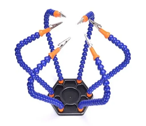
6 Flexible Arms Soldering Station With Swiveling Alligator Clip
Hold your PCB securely during post-reflow inspection and rework. The 6-arm helping hands keeps the board at any angle while you work with tweezers and an iron for touch-up joints.

0.1MM Copper Soldering Solder PPA Enamelled Repair Reel Wire
Fine enamelled copper wire for repairing lifted PCB traces after rework. Use to bridge damaged tracks from tombstoned component pads — nearly invisible once soldered in place.
Frequently Asked Questions
Q: Can I reflow both sides of a PCB?
Yes — this is called double-sided reflow. Solder the bottom side first (typically only light components like resistors and capacitors). When you reflow the top side, gravity wants to pull the bottom components off, but surface tension in the molten solder holds them in place — as long as the component weight doesn’t exceed the surface tension force. As a rule of thumb: components lighter than 30g per square centimetre of pad area stay in place during a second reflow pass.
Q: How do I know if my hot plate temperature is correct?
Use a K-type thermocouple (from a digital multimeter with thermocouple input) taped flat to the PCB surface to monitor actual board temperature — not hot plate temperature, which can differ significantly. An IR thermometer also works but is less accurate on shiny PCB surfaces (emissivity correction needed). Apply a small piece of black electrical tape and measure on that spot for better IR accuracy.
Q: What’s the minimum component size I can reflow on a hot plate?
A hot plate can handle any passive size from 0201 upwards, and ICs from SOT-23 to large QFP packages. The limitation is component placement accuracy — smaller components are harder to place accurately by hand. For 0402 and smaller, a microscope or high-magnification loupe is needed for placement verification before reflow. QFN packages with bottom pads (thermal slugs) reflow well on a hot plate and are actually easier on a plate than with a hot air gun alone.
Q: Why do solder balls form during reflow?
Solder balls form when paste solvent evaporates too quickly (too-fast ramp rate) or when paste is applied on solder mask rather than on pads. The flux boils before the solder melts, spattering tiny solder spheres. Fix: slow down the ramp rate, ensure paste is only on pads, and check that your paste is fresh (old paste has degraded flux).
Q: Is hot plate reflow safe indoors?
Solder paste releases flux fumes during reflow — these are irritating to the respiratory system. Always work with good ventilation: open windows, a fan blowing fumes away from you, or a DIY fume extractor (a PC fan through an activated carbon filter works well). Lead-based paste requires additional care — clean the hot plate surface and work area after use, and wash hands before eating. A dedicated workshop area is ideal, but a ventilated kitchen or balcony works for occasional use.
Take Your PCB Assembly to the Next Level
Whether you’re assembling your first SMD prototype or building small production runs, Zbotic.in has the components, capacitors, resistors, and soldering tools you need. Shop our full range of electronics components with fast delivery across India and build with confidence.


Add comment