
PCB Gerber Files: From KiCad Design to Manufacturer
If you’ve ever designed a printed circuit board, you know the moment of truth: generating PCB Gerber files from KiCad and sending them off to a manufacturer. Gerber files are the universal language of PCB fabrication — without them, your beautifully designed board stays trapped on screen. In this guide, we walk through the complete workflow: from finishing your KiCad schematic, through Gerber generation, to placing your order with a manufacturer. Whether you are a first-time maker or an experienced hobbyist levelling up your electronics game, this tutorial covers everything you need to know.
What Are Gerber Files and Why Do They Matter?
Gerber files are industry-standard file formats (RS-274X, also called Extended Gerber) that describe every physical layer of your PCB. Think of them as a precise blueprint: each file tells the PCB manufacturer exactly where copper traces go, where the solder mask is applied, where silkscreen markings are printed, and where holes need to be drilled.
The Gerber format was originally developed by Gerber Scientific in the 1960s. Today, the RS-274X variant is universally accepted by fabrication houses worldwide — from budget services like JLCPCB and PCBWay to premium manufacturers. When you say “I am going to fab my board,” you almost always mean “I am going to send Gerber files.”
A typical Gerber package includes multiple files:
- F.Cu / B.Cu — Front and back copper layers
- F.Mask / B.Mask — Solder mask layers (where solder paste goes)
- F.SilkS / B.SilkS — Silkscreen (component labels, logos)
- F.Courtyard / B.Courtyard — Clearance boundaries
- Edge.Cuts — Board outline
- *.drl — Drill files (Excellon format)
Each file is a plain text description of shapes, lines, and flashes. Manufacturers feed these into automated optical inspection (AOI) machines and CNC routing equipment to produce your board.
KiCad PCB Design Basics: Getting Ready
KiCad is a free and open-source EDA (Electronic Design Automation) suite that has become the go-to choice for hobbyists and professionals alike. Before generating Gerbers, your KiCad project needs to be in order.
Schematic First, PCB Second
Always start with the schematic in KiCad Eeschema. Add all components, assign footprints, and generate a netlist. Skipping proper footprint assignment is the single most common cause of board rework orders from first-time makers.
Footprint Assignment Tips
- For through-hole resistors and capacitors, use the standard 2.54mm pitch footprints
- For SMD components, double-check land pattern dimensions against the datasheet
- Use KiCad 3D viewer to visually confirm component fit before Gerber export
- Check your IPC-7351 land pattern standard for production boards
Setting Up Board Stackup
In KiCad PCBnew, go to Board Setup then Board Stackup. For a standard 2-layer board, you will have F.Cu, Dielectric (FR4), and B.Cu. Set your dielectric thickness to 1.6mm for standard boards — the most common and cheapest option at Indian manufacturers.
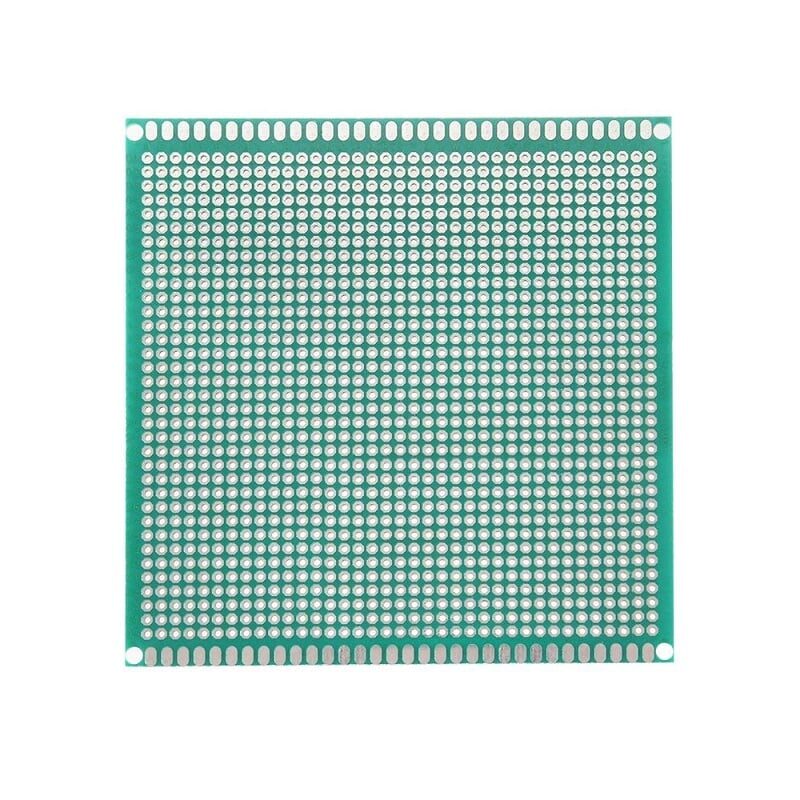
10 x 10 cm Universal PCB Prototype Board Single-Sided 2.54mm
Perfect for prototyping your circuit before committing to a custom PCB order. Standard 2.54mm pitch matches most through-hole components.
Generating Gerber Files in KiCad (Step-by-Step)
Here is the exact procedure for KiCad 7.x and 8.x (the current stable versions as of 2025):
Step 1: Open the Plot Dialog
In PCBnew, go to File then Plot (or press Ctrl+Shift+P). The Plot dialog opens.
Step 2: Select Output Format
From the Plot format dropdown, select Gerber. This is the default and correct choice for PCB manufacturers.
Step 3: Choose Output Directory
Set your output directory — create a folder called gerbers/ inside your project directory. Keeping Gerbers separate makes zipping and sending clean.
Step 4: Select Layers to Plot
Check all relevant layers. At minimum for a 2-layer board:
- F.Cu (front copper)
- B.Cu (back copper)
- F.Paste (front solder paste — needed if doing SMT reflow)
- B.Paste (back solder paste)
- F.Silkscreen
- B.Silkscreen
- F.Mask
- B.Mask
- Edge.Cuts (board outline — absolutely required)
- F.Courtyard (optional but recommended)
Step 5: Configure Plot Options
Enable these critical options:
- Use Protel filename extensions — Most manufacturers prefer this (gives files like .GTL, .GBL, .GTS, .GBS, etc.)
- Generate Gerber job file — Creates a .gbrjob metadata file
- Check zone fills before plotting — Ensures copper pours are up to date
- Coordinate format: 4.6 — Gives you 1nm resolution, more than adequate
Step 6: Click Plot
Hit the Plot button. KiCad generates one file per selected layer into your output directory.
Step 7: Generate Drill Files
Do not close the Plot dialog yet! Click Generate Drill Files. In the drill dialog:
- Format: Excellon (universally supported)
- Units: Millimeters
- Zeros format: Suppress leading zeros
- Drill origin: Absolute
Click Generate Drill File. You will get a .drl file (or separate PTH/NPTH files for plated vs non-plated holes).
Step 8: Zip Everything
Select all files in your gerbers/ folder and create a ZIP archive. Name it something descriptive like MyBoard_v1.0_Gerbers.zip. This ZIP is what you upload to the manufacturer.
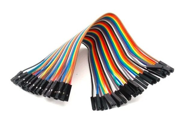
10CM Female To Female Breadboard Jumper Wires 2.54MM – 40Pcs
Use these for quick breadboard prototyping while your PCB is being manufactured. Saves time during the fabrication wait.
Understanding Each Gerber Layer
New designers often get confused about what each Gerber layer actually does. Here is a clear breakdown:
| File Extension | Layer Name | Purpose |
|---|---|---|
| .GTL | Top Copper | All copper traces and pads on top layer |
| .GBL | Bottom Copper | Copper on bottom layer |
| .GTS | Top Solder Mask | Green (or other colour) coating; openings expose pads |
| .GTO | Top Silkscreen | Component designators, logos, and text |
| .GKO / Edge.Cuts | Board Outline | Tells the router where to cut the board |
| .DRL | Drill File | X/Y coordinates and diameters of all holes |
Always verify your Gerbers using a free Gerber viewer before uploading. gerbv (open source) and the online viewers at JLCPCB or PCBWay work great. Many beginners have paid for boards only to find a missing layer or misaligned silk.
Drill Files, BOM, and Pick-and-Place
A complete manufacturing package includes more than just Gerbers:
Drill Files (Excellon)
KiCad generates these alongside Gerbers. They are in Excellon format (.drl) — a separate standard that describes hole locations. Some manufacturers want PTH (plated through holes) and NPTH (non-plated, like mounting holes) as separate files. KiCad can generate both.
Bill of Materials (BOM)
For SMT assembly services, you will need a BOM. In KiCad, go to Tools then Generate Bill of Materials. Export as CSV. The BOM maps each component reference (R1, C3, U1) to its part number and value.
Pick and Place File (CPL)
If ordering SMT assembly, the manufacturer also needs a Component Placement List. In KiCad, go to File then Fabrication Outputs then Component Placement (.pos). This gives X/Y coordinates and rotation for every SMT component.
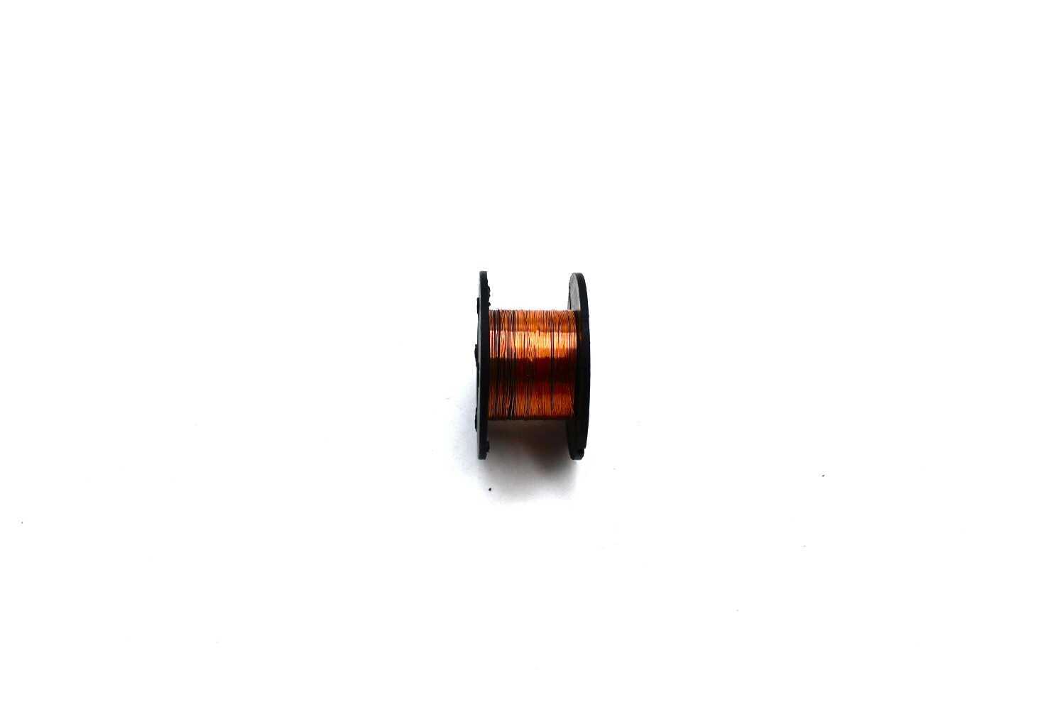
0.1MM Copper Soldering Solder PPA Enamelled Repair Reel Wire
Ultra-thin enamelled wire ideal for PCB rework, jumper wires, and manual trace repairs on your custom boards.
Design Rule Checks (DRC) Before Sending
Never send Gerbers without running DRC first. KiCad Design Rule Check catches errors that would either cause manufacturer rejections or result in a non-functional board.
Running DRC in KiCad
Go to Inspect then Design Rules Checker. Click Run DRC. Investigate every error and warning. Common DRC violations include:
- Clearance violations — Traces too close together (minimum 0.2mm for most budget fabs)
- Annular ring too small — The copper ring around a via or through-hole pad is too narrow
- Hole too small — Many budget manufacturers cannot drill below 0.3mm reliably
- Unconnected nets — Ratsnest lines still present; traces not connected
- Copper outside board edge — Copper extends beyond Edge.Cuts layer
Manufacturer Design Rules
Check your manufacturer capabilities page before designing. Common specs for budget Indian/Chinese fabs:
- Minimum trace width: 0.1mm (but 0.15mm is safer)
- Minimum clearance: 0.1mm (use 0.2mm for reliability)
- Minimum via drill: 0.3mm
- Minimum hole size: 0.3mm
- Board thickness: 0.8mm, 1.0mm, 1.2mm, 1.6mm (1.6mm is standard)
Choosing a PCB Manufacturer in India
You have several solid options for Indian makers ordering PCBs in 2025:
International (Ship to India)
- JLCPCB — $2 for 5 boards (100x100mm, 2-layer). Ships DHL to India in 5-7 days. Most popular among Indian hobbyists.
- PCBWay — Slightly more expensive but better customer service. Good for 4-layer and special finishes.
- Elecrow — Good for combined PCB+assembly orders.
Domestic (India)
- PCBPower (Gujarat) — Fast turnaround, INR billing, GST invoice
- Nextpcb — Has an India office, slightly faster customs than pure Chinese fabs
- Razorboard / Greenpcb — Indian domestic options, good for urgent orders
What to Check Before Ordering
Confirm these before uploading your ZIP:
- Board dimensions and layer count match your design
- Copper weight (1oz/35 micrometres for most hobbyist boards)
- Surface finish: HASL (cheapest), ENIG (gold, better for fine-pitch SMD)
- Solder mask colour: Green (default/cheapest), Red, Blue, Black available
- Silkscreen colour: White (default)

6 Flexible Arms Soldering Station With Swiveling Alligator Clip
Hands-free soldering helper with 6 flexible arms and alligator clips — essential when populating your freshly arrived custom PCB.
Frequently Asked Questions
Q: What is the difference between Gerber RS-274D and RS-274X?
RS-274X (Extended Gerber) is the modern standard and includes aperture definitions inside each file. RS-274D (the old standard) requires a separate aperture file. Always use RS-274X — KiCad defaults to this and all modern manufacturers expect it.
Q: Do I need to include the .GBR job file in my ZIP?
It is optional but helpful. The .gbrjob file provides metadata about your board (layer stackup, board revision, etc.) that some advanced CAM software can use. Including it does not hurt; most fabs simply ignore it if they do not need it.
Q: Why does my manufacturer say “missing board outline”?
You forgot to include or plot the Edge.Cuts layer. This layer defines the board physical outline. Without it, the manufacturer does not know where to route/cut the board. Re-plot and include Edge.Cuts (sometimes labelled as .GKO in Protel naming).
Q: Can I modify the Gerber files directly after generating them?
Technically yes — Gerbers are text files — but it is strongly discouraged. Any modification should be done back in KiCad and the Gerbers regenerated. Directly editing Gerbers is error-prone and version control becomes a nightmare.
Q: How many copies should I order for a first prototype run?
Order at least 5 pieces (which is the minimum at most budget fabs and usually costs the same as 1 piece). This gives you spares for debugging, rework mistakes, and sharing with collaborators. If you are confident in your design, 10 pieces is a reasonable quantity for a first functional prototype.
Ready to start your PCB journey? Zbotic.in stocks all the components you need — from prototyping boards and jumper wires to resistors, capacitors, and sensors. Browse the full collection and get everything delivered across India.


Add comment