
In power electronics, no design decision is more consequential than the choice of switching device. Whether you are building a motor drive, an inverter, a switching power supply, or a battery charger, the battle almost always comes down to two candidates: the IGBT (Insulated Gate Bipolar Transistor) and the power MOSFET.
Both are voltage-controlled, gate-insulated switches with high input impedance. Both can handle hundreds of amperes. But their internal physics differ fundamentally, leading to trade-offs in voltage rating, switching speed, conduction loss, and thermal performance that directly determine which one belongs in your circuit.
This is a thorough, no-shortcuts guide to the IGBT vs MOSFET decision — covering physics, datasheet parameters, switching waveforms, thermal modelling, and practical application rules.
1. MOSFET Physics and Structure
A power MOSFET is a unipolar device — conduction occurs through a single carrier type (electrons for N-channel, holes for P-channel). The key structure is the vertical DMOS (Double-diffused Metal Oxide Semiconductor) cell:
- A thin gate oxide controls a channel between the source and drain body
- When VGS exceeds the threshold voltage (typically 2–5V for enhancement mode), an inversion channel forms, allowing current to flow
- The drain-to-source resistance when ON (Rds(on)) is the primary loss mechanism
Because conduction is purely resistive (majority carriers only), MOSFETs switch extremely fast — rise and fall times of tens of nanoseconds are routine. There are no minority carriers to store or recombine, so no tail current on turn-off.
The main physical constraint is the body diode — an intrinsic anti-parallel diode formed by the DMOS structure. This is often exploited in synchronous rectification and half-bridge circuits.
MOSFET Figure of Merit: Rds(on) × Qg
The best single metric for comparing MOSFETs is Rds(on) × Qg (gate charge). Lower is better. This product captures the trade-off between conduction loss and switching speed — modern super-junction MOSFETs optimise this trade-off aggressively.
2. IGBT Physics and Structure
The IGBT is a hybrid device that combines a MOSFET input structure (high input impedance, voltage-controlled gate) with a BJT output structure (bipolar current conduction). It was developed in the 1980s specifically to overcome the high Rds(on) of high-voltage MOSFETs.
Structurally, an IGBT has:
- A MOSFET-like gate structure that controls a channel
- A P+ substrate at the collector (equivalent to a PNP transistor’s emitter)
- When the gate turns on, the MOSFET channel carries electrons, which then forward-bias the P+ collector injection, flooding the drift region with holes (conductivity modulation)
This conductivity modulation dramatically reduces the on-state voltage drop (Vce_sat ≈ 1.0–2.5V) regardless of device voltage rating. A 1200V IGBT has essentially the same Vce_sat as a 600V IGBT — whereas a 1200V MOSFET has an Rds(on) roughly 4× higher than a 600V MOSFET due to the drift layer physics.
The price of conductivity modulation: the stored minority carriers must be removed on turn-off. This creates a characteristic current tail that limits switching frequency and generates switching losses.
3. Key Datasheet Parameters Compared
| Parameter | Power MOSFET | IGBT |
|---|---|---|
| On-state voltage model | V = I × Rds(on) | V = Vce_sat (flat, ~1.5–2.5V) |
| Input impedance | Very high (voltage controlled) | Very high (voltage controlled) |
| Threshold voltage (Vth) | 2–5V typical | 4–6V typical |
| Max switching frequency | Up to several MHz | Typically <50kHz (older), <150kHz (modern trench-gate) |
| Voltage range (common) | Up to ~900V practically | 600V–6.5kV |
| Current range | Milliamps to hundreds of A | 5A to >3600A (modules) |
| Body diode | Intrinsic (fast or slow) | Not usable (slow, high V_f) |
| Negative temp coefficient (saturation current) | Positive (Rds(on) rises with temp → easier paralleling) | Positive Vce_sat at high current → acceptable paralleling |
| Cost (at equivalent rating) | Higher above ~600V | Lower above ~600V |
4. Conduction Losses: Rds(on) vs Vce(sat)
This is the heart of the IGBT vs MOSFET trade-off. The two devices model their on-state losses differently:
MOSFET Conduction Loss
P_cond = I_RMS² × Rds(on)
Example: 20A RMS through 50mΩ MOSFET → P = 400 × 0.05 = 20W
Because Rds(on) scales approximately as V_BR^2.5 (for conventional planar MOSFETs), a 1200V MOSFET has ~100× higher Rds(on) than a 200V device at the same die size. This makes high-voltage MOSFETs very lossy at high current.
IGBT Conduction Loss
P_cond = Vce_sat × I_C (for square wave)
Example: 20A through IGBT with Vce_sat=2V → P = 2 × 20 = 40W
The IGBT’s conduction loss is independent of voltage rating. A 1200V IGBT and a 600V IGBT at the same chip size have nearly the same Vce_sat. This is the IGBT’s defining advantage at high voltages.
The Crossover Point
The crossover where IGBT becomes superior in conduction loss occurs when:
I² × Rds(on)_MOSFET > Vce_sat_IGBT × I
I > Vce_sat / Rds(on)_MOSFET
For a 600V MOSFET with Rds(on)=100mΩ and a comparable IGBT with Vce_sat=2V:
Crossover: I = 2V / 0.1Ω = 20A
Below 20A, the MOSFET has lower conduction loss. Above 20A, the IGBT wins. This crossover calculation should be your starting point for any high-current design decision.
5. Switching Losses and Frequency Limits
Switching loss is the energy dissipated during each transition (turn-on and turn-off) times the switching frequency:
P_sw = (E_on + E_off) × f_sw
IGBT turn-off creates a current tail — even after the gate voltage is removed, stored minority carriers continue to flow for 0.1µs–several µs depending on IGBT technology:
- Punch-through (PT) IGBTs: Fast, but higher conduction losses. Common in older designs.
- Non punch-through (NPT) IGBTs: Lower conduction loss, slightly slower. Better thermal characteristics.
- Trench-gate field-stop IGBTs (modern): Both fast switching AND low conduction loss. The current generation of IGBT technology (e.g., Infineon IKW/IKFW series, ON Semiconductor NGx series).
Practical frequency limits:
- Conventional IGBTs: 20kHz–50kHz (industrial motor drives, UPS, solar inverters)
- Fast IGBTs: 50kHz–150kHz (switching power supplies, high-frequency induction heating)
- Power MOSFETs: 100kHz–10MHz (SMPS, resonant converters, RF amplifiers)
For audio-frequency motor drives (1kHz–20kHz), IGBTs at 600V–1200V are dominant. For high-frequency DC-DC converters (200kHz+), MOSFETs are the only viable choice.
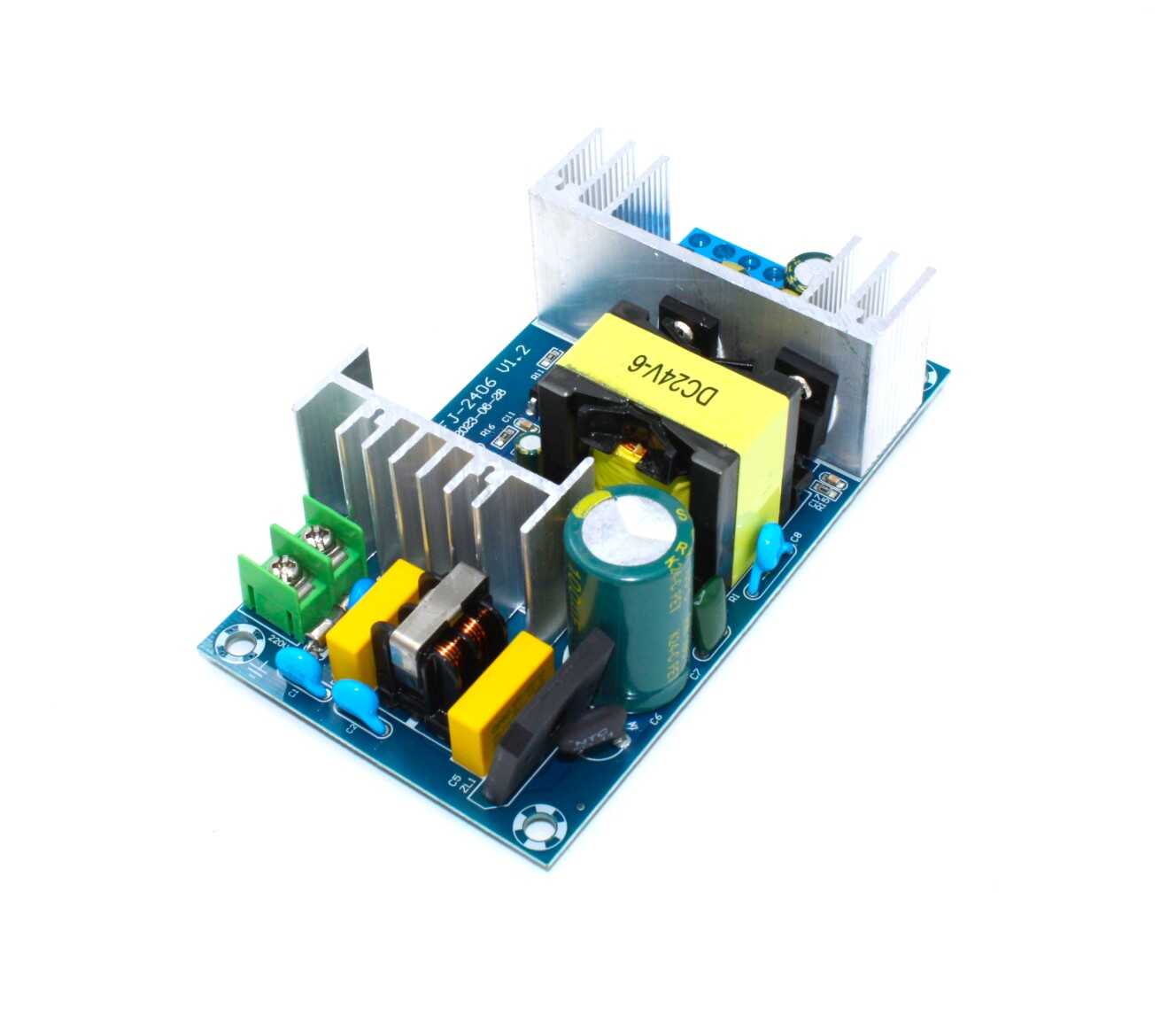
150W AC-DC Buck Converter – 100V-240V to 24V
A ready-made power supply module that uses optimised power switching internally. Study the design or use it to power your IGBT/MOSFET test circuits.
6. Gate Drive Requirements
Both IGBTs and MOSFETs have capacitive gate inputs. The gate charge (Qg) determines how much charge must be moved to fully turn the device on or off, and directly affects switching speed and gate driver power:
Gate driver power: P_gate = Qg × Vgs × f_sw
Example: Qg=100nC, Vgs=15V, f_sw=50kHz → P = 100e-9 × 15 × 50e3 = 75mW
MOSFET Gate Drive
- Drive voltage: 10–15V for reliable full enhancement (logic-level MOSFETs can use 4.5–5V)
- Turn-off: Drive to 0V (or negative for fast turn-off and latch-up prevention)
- Typical Qg: 5nC–200nC for standard devices; 10nC–50nC for fast switching types
IGBT Gate Drive
- Drive voltage: +15V for turn-on (never exceed Vge_max, typically ±20V)
- Turn-off: Drive to –5V to –15V (negative bias critical for preventing spurious turn-on during fast dv/dt)
- Typical Qg: 50nC–500nC (higher than equivalent MOSFETs due to Miller plateau)
- Never drive an IGBT gate with a bare Arduino — always use a dedicated gate driver IC (IR2110, 1EDC20I12MH, TLP350)
The gate resistor (Rg) controls dv/dt and di/dt. Larger Rg = slower switching = lower EMI but higher switching losses. Typical values: 4.7Ω–47Ω for IGBTs, 2.2Ω–22Ω for MOSFETs.
7. Thermal Performance and Safe Operating Area
Junction-to-Case Thermal Resistance (Rth_jc)
Total power dissipation = conduction + switching losses. This must be removed via the heatsink:
Tj = Tc + P_total × Rth_jc
Max Tj for Si devices: 150°C–175°C
Design target: Tj_max = 125°C (25°C headroom)
MOSFET Thermal Advantage
MOSFETs have a positive temperature coefficient of Rds(on) — as they heat up, Rds(on) increases, reducing current. This inherent negative feedback makes multiple MOSFETs easier to parallel (current naturally distributes evenly). IGBTs also parallel well due to the positive temperature coefficient of Vce_sat at high current levels.
Safe Operating Area (SOA)
The SOA graph defines the safe combinations of VDS (or VCE) and ID (or IC) at various pulse widths. IGBTs generally have better SOA than equivalent MOSFETs at high voltages — they can withstand the simultaneous application of high voltage and high current for longer during hard switching. This matters for motor drives where shoot-through or load shorts can subject the device to extreme stress.
8. Voltage and Current Range Selection
The voltage rating of your application is the most direct pointer to which device to use:
Under 100V
Always MOSFET. Rds(on) is extremely low (sub-milliohm for large devices), switching is fast, and cost is low. IGBTs are not manufactured for voltages below ~200V — their conductivity modulation mechanism becomes counter-productive at low voltages.
100V–400V
Usually MOSFET for moderate currents (<30A). At higher currents, evaluate the crossover calculation. 200V super-junction MOSFETs (CoolMOS) have revolutionised efficiency in this range — sub-20mΩ at 600V is now achievable.
400V–1200V
Contested territory. For frequencies above 50kHz, fast MOSFETs (SJ-MOS, GaN in the future). For frequencies below 20kHz at currents above 20–30A, IGBTs win on conduction loss. Motor drives and inverters almost universally use IGBTs here.
Above 1200V
Always IGBT (or SiC MOSFET at premium cost). High-voltage MOSFETs above 1200V have prohibitively high Rds(on) due to the thick drift layer required for blocking voltage. IGBTs scale beautifully to 6.5kV for rail traction and HVDC applications.
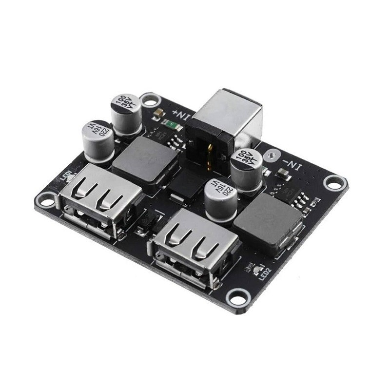
2 Channel USB QC3.0/QC2.0 DC-DC Buck Converter Module
A practical MOSFET-based switching converter module for 6–32V input to fast-charge USB outputs. See MOSFET switching in a real application.
9. Application-by-Application Guide
| Application | Recommended Device | Reason |
|---|---|---|
| Arduino DC motor driver (12V, 2A) | N-channel MOSFET (IRLZ44N) | Low voltage, low current, logic-level gate |
| PWM LED dimmer (12–24V, 10A) | N-channel MOSFET (IRF3205) | High frequency PWM, low voltage, resistive load |
| Solar inverter (230V AC output, 5kW) | IGBT module (600V/50A) | High voltage, medium frequency (10–20kHz), high current |
| SMPS (5V/3A from mains) | MOSFET (650V super-junction) | High frequency (100kHz+) — IGBT too slow |
| 3-phase AC motor drive (400V, 10kW) | IGBT module (1200V/50A) | Standard industrial choice; switching at 4–16kHz |
| Buck converter (48V to 12V, 20A) | N-channel MOSFET (80V, low Rds) | Low voltage, high frequency, low conduction loss |
| Induction heater (resonant, 25kHz) | Fast IGBT or MOSFET | Depends on bus voltage; IGBT for 300V+, MOSFET below |
| EV motor controller (400V DC bus) | IGBT module (1200V/600A) | Industry standard; conductivity modulation handles huge current spikes |
10. Practical Circuit Design Tips
Decoupling and Snubbers
High-speed switching creates large dV/dt and dI/dt transients. Place low-ESR ceramic capacitors (100nF–10µF) directly across the power bus at the device. Snubber circuits (RC or RCD) clamp voltage spikes caused by parasitic inductance in the PCB layout.
PCB Layout Rules
- Minimise the loop area of the high-current switching loop (drain/collector → load → source/emitter → back to device)
- Keep gate drive traces short and away from high dV/dt nodes
- Use dedicated via stitching for ground planes under switching nodes
- Separate power and signal grounds; join at a single star point
Bootstrap Gate Drive for High-Side Switches
Driving the gate of a high-side N-channel MOSFET or IGBT requires the gate voltage to float above the source/emitter. Bootstrap gate driver ICs (IR2110, IR2104, FAN7392) provide this automatically using a bootstrap capacitor charged during low-side conduction.
Short Circuit Protection for IGBTs
IGBTs are vulnerable to desaturation under short circuit — the collector current rises uncontrollably, generating enormous power. Modern gate driver ICs include desaturation detection (monitoring Vce to detect when the IGBT leaves saturation) and initiate controlled soft turn-off to prevent destruction. Always implement this in motor drive and inverter designs.
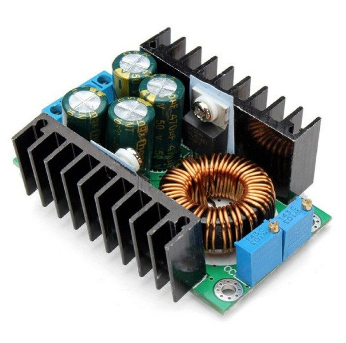
300W 10A DC-DC Step-Down Buck Converter Module
A 300W adjustable buck converter using a high-efficiency MOSFET-based topology — use this as a DC power source for IGBT/MOSFET test benches.
Frequently Asked Questions
Can I replace an IGBT with a MOSFET in an existing design?
Sometimes, but it requires careful analysis. Check voltage rating (the MOSFET must match or exceed the IGBT’s VCES), verify the MOSFET’s body diode speed if used in a bridge, recalculate gate drive requirements, and confirm conduction losses are acceptable. At high voltages (600V+), a direct MOSFET replacement for an IGBT will often have much higher Rds(on) and may overheat.
Why do IGBTs not have a body diode that can be used?
IGBTs do have an intrinsic diode, but it is slow (high reverse recovery charge, Qrr) and has a high forward voltage drop (~2V). Using it causes large current spikes and losses in bridge circuits. In IGBT modules, a separate anti-parallel fast-recovery diode (FRD) is always integrated for this reason.
What is SiC MOSFET and how does it compare?
Silicon Carbide (SiC) MOSFETs use SiC instead of silicon as the semiconductor material. SiC has ~10× higher breakdown field than Si, enabling high-voltage MOSFETs with much lower Rds(on) than equivalent Si devices. A 1200V SiC MOSFET competes directly with an IGBT in conduction loss while retaining MOSFET switching speed. Cost is 3–5× higher than Si IGBTs at present, but prices are falling rapidly. SiC is the future of the 600V–1700V power range.
What does "co-packed diode" mean in an IGBT module datasheet?
It means a fast-recovery anti-parallel diode is included in the same module package as the IGBT. This is standard in any IGBT intended for bridge circuits (inverters, motor drives). Single IGBT packages (TO-247) do not include this diode — you must add an external FRD in bridge configurations.
Can I parallel MOSFETs or IGBTs to increase current capacity?
Yes — both devices can be paralleled. MOSFETs paralleled well due to their positive Rds(on) temperature coefficient (current sharing is automatic). IGBTs also parallel reasonably well, but gate resistors (2–5Ω per device) should be used to prevent oscillation between paralleled devices. Match devices from the same manufacturer lot for best current sharing.
Conclusion
The IGBT vs MOSFET decision is not about one being universally better — it is about matching the device physics to your operating conditions. The golden rule: below 400V and above 50kHz, use a MOSFET. Above 600V and below 20kHz at high current, use an IGBT. In the overlapping region, calculate the conduction loss crossover current and let the numbers decide.
For most hobbyist projects — motor control, LED drivers, DC-DC converters operating at 12V–48V — a well-chosen N-channel power MOSFET will be the right answer almost every time. As you move into mains-voltage inverters, welders, or motor drives above a few kilowatts, IGBTs become the technically and economically correct choice.


Add comment