
Among all the disciplines in electronics design, proper grounding techniques for PCB layout remain the least taught and most frequently misunderstood. Yet grounding is what separates a circuit that barely works in a lab from one that performs reliably in a real-world deployment. Whether you are designing your first custom PCB for an Arduino project or tackling a mixed-signal audio board, understanding star ground, ground planes, and chassis grounding will dramatically improve your results. This guide covers all three in practical, actionable detail.
Table of Contents
- Why Grounding Techniques Matter on PCBs
- Star Grounding: The Fundamental Method
- Ground Plane: The Modern Standard
- Split Ground Planes for Mixed-Signal Boards
- Chassis Ground: Safety and Shielding
- Practical Grounding Tips for Indian Makers
- Recommended Products
- Frequently Asked Questions
Why Grounding Techniques Matter on PCBs
Ground is not just the zero-volt reference — it is the return current path for every signal and power current in your circuit. The way ground is implemented determines the impedance of these return paths, and impedance determines how much noise voltage is generated when currents flow.
Consider Ohm’s Law: V = I × R. Even a copper trace with 10mΩ of resistance will develop a 10mV voltage drop if 1A of current flows through it. If this current is a digital switching current (fast rise time), the inductance of the trace adds further voltage spikes. In a ground path shared by analog and digital circuits, this voltage fluctuation appears directly as noise at the analog circuit’s reference.
The goal of any grounding technique is to minimise the impedance (both resistive and inductive) of return current paths, and to prevent noisy return currents from sharing paths with sensitive circuits. Three primary approaches exist: star grounding, ground plane, and chassis ground — each suited to different circuit types.
Star Grounding: The Fundamental Method
Star grounding (also called single-point grounding) is the oldest and conceptually simplest grounding technique. In a star ground system, every ground connection in the circuit runs back to a single common node — the star point — rather than connecting to a daisy-chained ground bus.
How Star Grounding Works
Imagine a five-pointed star. The centre is your single ground reference point (often at the power supply’s negative terminal). Each arm of the star is a dedicated ground wire running to one section of your circuit: analog front-end, digital logic, motor driver, power amplifier, and power supply return. Because each section has its own dedicated path back to the star point, the return current of the noisy motor driver does not flow through the ground path of the sensitive analog section.
Advantages of Star Ground
- Prevents ground loops between sections
- Eliminates common-impedance coupling (where two sections share a ground path and one’s current creates noise for the other)
- Ideal for audio circuits, instrumentation amplifiers, and any circuit with sensitive analog sections alongside noisy loads
- Simple to implement on a perfboard or universal PCB with dedicated ground wires
Limitations of Star Ground
Star grounding becomes impractical at high frequencies (above a few MHz). At RF frequencies, even a few centimetres of wire has significant inductance, making the long dedicated ground runs from each section to the star point inductive — and therefore noisy at high frequencies. Star ground is primarily a low-frequency technique (DC to ~1MHz).
Also, on a densely populated PCB, running individual ground wires from every component back to a single point is physically impractical. Ground planes solve this problem.
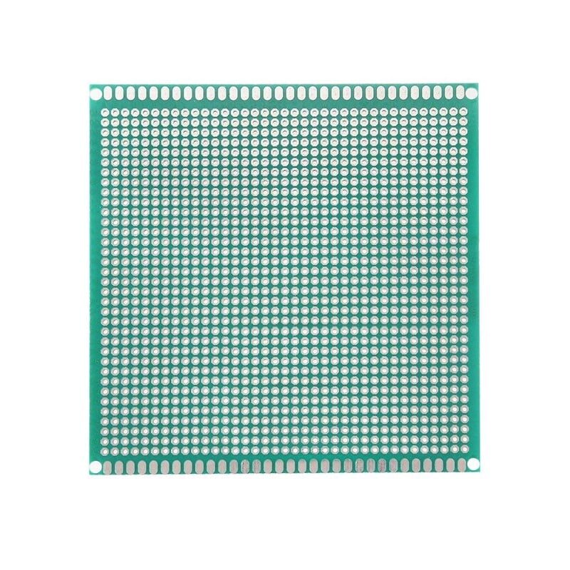
10 x 10 cm Universal PCB Prototype Board Single-Sided
Practice star grounding on this 10x10cm universal prototype PCB before committing to custom fabrication. Lay out dedicated GND traces from each circuit section to a central star point to see the noise reduction firsthand.
Ground Plane: The Modern Standard
A ground plane is a large, unbroken area of copper on a PCB layer dedicated entirely to ground. In a standard two-layer PCB, the top layer carries signal traces and the bottom layer is a solid ground plane. In four-layer PCBs, dedicated inner layers are used for power and ground planes.
Why Ground Planes Are So Effective
A solid copper plane has extremely low resistance (milliohms) and very low inductance because current can take the shortest possible path — directly below the signal trace that generated it. This is called the image plane effect: return current naturally flows in the ground plane directly beneath the signal trace, minimising the enclosed loop area and thus the inductance and radiation.
Key benefits of a ground plane:
- Low impedance return paths — return currents flow via shortest path, not through shared conductors
- EMI reduction — small loop areas mean less radiation and less susceptibility to external interference
- Controlled impedance — trace impedance over a ground plane is predictable, essential for high-speed signals
- Heat spreading — copper plane acts as a thermal spreader for power components
- Simpler layout — no need to route individual ground traces back to a star point
Ground Plane Best Practices
- Keep the plane solid: Avoid routing signal traces on the ground plane layer. Every slot or cut in the ground plane forces return current to detour around it, increasing inductance.
- Use vias generously: In multi-layer boards, place ground vias close to every component’s GND pad to connect it to the ground plane with minimal inductance.
- Avoid splitting the ground plane under high-speed signal traces: If a signal trace crosses from one section of the board to another, ensure the ground plane is continuous beneath it. A gap forces the return current to take a long detour.
- Thermal reliefs: On prototype boards, thermal relief spokes connect component pads to copper pours to make soldering easier without creating a massive heat sink. On production boards they may be reduced or eliminated.
Split Ground Planes for Mixed-Signal Boards
When a PCB contains both analog and digital sections — for example, a microcontroller with an ADC reading from a precision sensor — the question of how to handle the ground plane becomes more complex.
Digital circuits generate high-frequency switching noise in their ground return currents. If the analog and digital sections share a single continuous ground plane, these digital return currents flow through the same copper that forms the return path for analog signals — injecting noise into analog measurements.
The traditional solution was to split the ground plane into an analog ground (AGND) island and a digital ground (DGND) island, connected at a single point. This is essentially implementing star grounding at the PCB plane level. The one connection point between the two planes is typically at the power supply or at the ADC/DAC IC’s ground pin (which is usually the point at which the two domains interact).
However, modern guidance from IC manufacturers (including Texas Instruments and Analog Devices) often recommends a single unified ground plane even on mixed-signal boards, with careful placement: place analog circuitry in one region of the board and digital circuitry in another, and ensure no digital traces are routed over the analog region. The continuous plane provides lower impedance than a split plane with a single tie point, and the partitioning of the layout regions achieves the same goal of keeping digital return currents out of the analog area.
The best approach depends on your specific circuit. For very high precision (24-bit ADC, precision instrumentation), a carefully designed split plane may still be beneficial. For most hobbyist projects with 10-12 bit ADC resolution, a single plane with good partitioning works excellently.

0.1µF Ceramic Capacitor (Pack of 50)
Complement your ground plane design with 100nF ceramic decoupling capacitors at every IC power pin. Even the best ground plane benefits from local decoupling to handle transient current demands from switching ICs.
Chassis Ground: Safety and Shielding
Chassis ground (also called protective earth in Indian electrical codes) is the connection of the equipment’s metal enclosure to the earth ground conductor of the mains supply. It serves two distinct purposes:
Safety Function
In the event of a fault where a live (phase) conductor contacts the metal chassis, chassis grounding provides a low-impedance path to earth. This causes a large fault current to flow, which trips the circuit breaker or blows the fuse — protecting the user from electric shock. This is mandatory for all mains-powered equipment in India under IS standards.
The Indian mains supply uses a three-pin plug: Line (L, brown/red), Neutral (N, blue/black), and Earth (E, green/yellow). The earth pin connects to the building’s earth electrode system. Your equipment’s chassis must connect to this pin via the earth wire.
EMI Shielding Function
A grounded metal enclosure acts as a Faraday cage — it shields the internal electronics from external electromagnetic interference (like nearby radio transmitters, mobile phones, or industrial equipment) and prevents the internal electronics from radiating EMI that could interfere with nearby equipment. This is why high-quality audio equipment and precision instruments use metal enclosures connected to chassis ground.
Connecting Chassis Ground to Circuit Ground
In mains-powered equipment, chassis ground (earth) and signal/circuit ground (GND) are connected at a single point — usually at the power supply. This ensures no current flows through the chassis connection during normal operation (only during fault conditions). Never connect chassis ground to circuit ground at multiple points, as this creates a ground loop through the building’s earth network.
For battery-powered equipment in a metal enclosure, the chassis can still be connected to circuit ground for EMI shielding purposes, but there is no safety earth requirement since there is no mains voltage present.
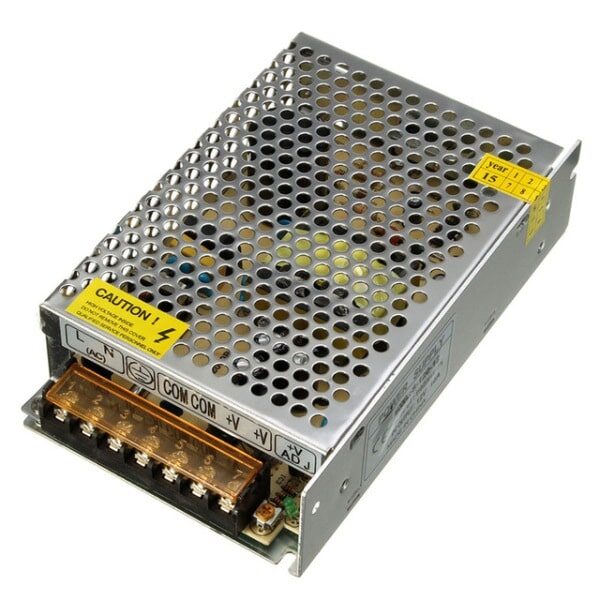
12V 10A SMPS – 120W – DC Metal Power Supply
A metal-enclosed SMPS with dedicated earth, neutral, and live terminals — ideal for learning chassis grounding in practice. The metal case provides built-in EMI shielding and can be chassis-grounded to your project enclosure for safety and noise reduction.
Practical Grounding Tips for Indian Makers
Here are ground-tested (pun intended) practical tips for Indian makers working with breadboards, prototype PCBs, and custom boards:
- Use dedicated black wires for GND on breadboards. Colour coding saves debugging time. Red = VCC, Black = GND. Never mix this up.
- On breadboards, use both GND rails. The top and bottom GND rails are separate — connect them together with a short black jumper wire at the start of every project.
- Tie all GNDs at the power supply, not at the load. Run ground wires from each module back to the power supply’s GND, not from module to module in a chain.
- Add a 100nF ceramic cap at every IC power pin. Non-negotiable for prototype PCBs. Do it before debugging anything else.
- Keep ground traces wide on perfboard/vero board. The wider the trace, the lower the resistance and inductance. For power ground carrying >500mA, use at least 2mm trace width (or doubled-up wire).
- Connect all GND pins of an IC. Many ICs (especially power ICs and digital logic) have multiple GND pins. All must be connected to ground, not just one.
- Separate your grounds before your project grows. It is much easier to implement star grounding from the start than to retrofit it after your circuit has ten modules.
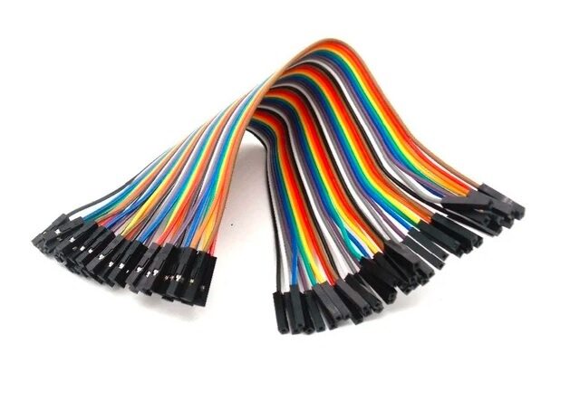
10CM Female To Female Breadboard Jumper Wires 2.54MM – 40Pcs
Keep a dedicated set of black F-F jumper wires specifically for all your ground connections. Using consistent colour coding on breadboards makes circuit debugging and review far faster.
Frequently Asked Questions
Q: Should I use star ground or a ground plane for my Arduino project?
For breadboard or perfboard Arduino projects at low frequencies (DC sensors, slow communication), star grounding with dedicated GND wires from each module to the Arduino’s GND pin works well. If you are designing a custom PCB, use a solid ground plane — it provides better performance with less design effort.
Q: My PCB has a ground pour but I still have noise — what am I missing?
Check for: (1) splits or cuts in the ground plane under signal traces, (2) missing decoupling capacitors or caps placed too far from IC power pins, (3) high-current traces (motor drive, relay) running near sensitive analog traces on the top layer. Also check that all GND pads are properly connected to the plane via thermal reliefs or direct connections.
Q: What is the difference between AGND and DGND on an ADC IC datasheet?
AGND is the ground reference for the ADC’s analog circuits (reference voltage, sample-and-hold). DGND is the ground reference for its digital interface (SPI/I2C outputs). These are often separate pins precisely so you can connect them to different ground planes. For most hobbyist projects, both can connect to the same ground plane if digital switching noise is managed with decoupling capacitors.
Q: Is chassis grounding required for a battery-powered project?
Not for safety (no mains voltage involved), but you can still connect the chassis to circuit GND for EMI shielding. This is optional for most hobbyist projects unless RF interference from nearby equipment is causing problems.
Q: How do I implement star grounding on a breadboard?
Choose one GND rail column as your star point. Run individual black jumper wires from the GND pin of each module directly to this column, rather than chaining them (Module A GND → Module B GND → Module C GND). This gives each module its own dedicated return path to the common star point.
Take your circuit design to the next level. Find prototype PCBs, capacitors, resistors, jumper wires, and power supplies at Zbotic Electronics Components — quality parts, fast delivery across India.


Add comment