
Electromagnetic Compatibility: Reduce RF Noise in PCB Design
Designing a PCB that passes EMC and RF noise reduction tests is one of the biggest challenges for Indian electronics engineers and advanced makers. Whether you are building a wireless sensor, a motor controller, or an IoT gateway, unwanted electromagnetic interference can corrupt data, reduce radio range, trigger false resets, or cause your product to fail BIS certification in India. The good news is that most EMC problems are solvable at the PCB layout stage — and many of the fixes cost nothing beyond careful design decisions. This guide covers the most impactful techniques used by professionals.
EMC Fundamentals: How RF Noise is Generated
Every time current changes direction or magnitude — which happens billions of times per second in a digital circuit — it generates electromagnetic radiation. The faster the edge rate (how quickly a logic signal transitions from low to high), the broader the frequency spectrum of the emission. A 3.3V signal with a 1ns rise time radiates harmonics well into the GHz range.
There are two coupling mechanisms to control:
- Conducted emissions: Noise that travels along power and signal wires, potentially interfering with other devices on the same supply or signal bus.
- Radiated emissions: Noise that propagates as electromagnetic waves through space, interfering with nearby wireless receivers — your NRF24L01, ESP32 Wi-Fi, or GPS module.
The loop area of current paths is the most important factor in radiated emissions. Large current loops act like antennas. The formula is simple: minimise loop area = minimise emissions. Everything else in EMC design flows from this principle.
Ground Plane Design: The Single Most Important Rule
A continuous, unbroken copper ground plane on the inner layer (for 4-layer boards) or bottom layer (for 2-layer boards) is the most impactful EMC improvement you can make. The ground plane provides a low-impedance return path for every signal on the board, minimising current loop area automatically.
Critical rules for ground planes:
- Never split the ground plane under digital circuits unless you specifically need to isolate analogue ground. Even then, connect AGND and DGND at a single point near the ADC. A split ground plane forces return currents to take long detour paths, creating large current loops and massive radiation.
- Avoid slots and cuts. Every trace that crosses a slot in the ground plane forces the return current to go around the slot — creating a large loop. Route all high-speed signals such that their return path on the ground plane is direct and unobstructed.
- Star grounding for power converters. Connect all switching converter grounds back to a central star point, not daisy-chained. Daisy-chaining carries switching noise across the entire board.
- Stitch vias. On multi-layer boards, use via stitching (vias connecting ground planes on different layers) along the board perimeter and around RF modules. Spacing should be less than λ/20 at the highest frequency of concern.
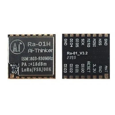
Ai Thinker LoRa Ra-01H Module
LoRa modules are extremely sensitive to PCB layout. The Ra-01H operates at 868 MHz and requires careful antenna keep-out implementation for reliable long-range performance.
Decoupling Capacitors: Placement and Value Selection
Decoupling capacitors suppress power supply noise at the IC level by providing a local reservoir of charge. When an IC’s output switches, the current demand spike is supplied by the nearby capacitor rather than travelling all the way back through the PCB traces and power supply — reducing the effective current loop area.
Placement is more important than value: A 100nF capacitor placed 5mm from an IC pin is more effective than a 10µF capacitor placed 20mm away. The goal is to minimise the distance between the capacitor and the IC’s VCC and GND pins.
Standard decoupling strategy:
- Place one 100nF ceramic (X7R) capacitor within 1–2mm of each VCC pin of every IC
- Add one 1µF–10µF bulk capacitor per power rail per IC cluster
- For MCUs like ESP32 and STM32 with multiple VCC/VDDA pins, decouple each pin separately
- Use via-in-pad or place the capacitor directly on the VCC-GND trace to minimise inductance
- Avoid using electrolytic capacitors for high-frequency decoupling — their high ESR makes them ineffective above ~1 MHz. Use ceramic (MLCC) capacitors
Common mistake: Routing the trace from VCC to the IC first, then branching off to the decoupling capacitor. Instead, route VCC → capacitor → IC pin. This ensures the capacitor is always between the supply and the IC load.
Trace Routing for RF and High-Speed Signals
Every trace on a PCB is a transmission line. For signals above approximately 30 MHz (or with edge rates faster than ~10ns), impedance matching becomes important.
Key routing rules:
- Keep high-speed traces short and direct. Every extra millimetre adds inductance and potential radiation.
- Avoid right-angle bends (90°). Use 45° angles or curves. Right angles change the effective trace width at the corner, creating impedance discontinuities and spurious radiation. Modern EDA tools enforce this automatically.
- Route differential pairs together. USB, Ethernet, and differential clock signals should have matched lengths (±0.1mm) and constant spacing. The differential signal cancels its own magnetic field, drastically reducing radiation.
- Keep analogue and digital traces separate. Analogue signal traces should never run parallel to clock or PWM traces. If they must cross, do so at 90° angles to minimise capacitive coupling.
- Clock traces deserve a guard ring. Surround high-speed clock traces with a guard trace connected to ground at both ends. This creates a Faraday-cage effect that contains the field.
Wireless Module Keep-Out and Antenna Placement
This section is critical for Indian makers designing custom PCBs that incorporate wireless modules like NRF24L01, ESP32, LoRa, or GSM modules.
Antenna keep-out zone: The area beneath and around the module’s antenna must have no copper — not even ground plane. Most module datasheets specify this keep-out area explicitly. For PCB trace antennas (common on ESP32, ESP8266, and NRF24L01), this means a copper-free zone extending at least 3mm below and to the sides of the antenna trace, and the antenna should overhang the PCB edge.

Ai Thinker LoRa Ra-01SC Module
The Ra-01SC uses a ceramic chip antenna with a defined keep-out area in its datasheet — ideal for compact PCB designs where an external whip antenna is impractical.
External antenna via U.FL/IPEX connector: If your PCB must have a ground plane edge-to-edge, use a module with a U.FL connector and route a cable to an external antenna. This completely eliminates the keep-out constraint. Use a 50Ω impedance-controlled trace from the module’s RF output to the connector.

15cm 3DBI GSM/GPRS/3G PCB Antenna with IPEX Connector
A flexible PCB antenna with IPEX connector — mount it away from noisy PCB areas to maximise wireless module sensitivity and bypass keep-out zone constraints entirely.
Power Supply Noise Reduction
Switching power supplies (buck converters, boost converters) are among the most significant sources of conducted and radiated EMI on a PCB. Their switching transients generate harmonics that can span from DC to several hundred MHz.
Layout rules for switch-mode supplies:
- Keep the hot loop (input cap → switch → inductor → output cap) as small as possible — place components tightly
- The switch node trace should be short and wide, but never exposed as a large copper pour (it becomes an antenna)
- Place a common-mode choke on the input power line to suppress conducted noise
- Add an LC filter on the output of every switching supply before routing to sensitive circuits (wireless modules, analogue sensors)
- For linear regulators (LDO): even though LDOs are quieter than switching supplies, they still need proper decoupling. Place 100nF + 10µF at both input and output
Simple EMC Pre-Testing Without a Shielded Room
Professional EMC testing at an accredited lab in India costs ₹50,000–₹2,00,000 per test run. For prototyping, you can do pre-compliance testing cheaply:
- Near-field probe + oscilloscope: A DIY near-field probe (a small coil of wire connected to an oscilloscope or spectrum analyser input through a 50Ω terminator) can identify the noisiest areas on your PCB. Hover it over the board and watch the spectrum change.
- RTL-SDR dongle as spectrum analyser: An RTL-SDR (₹1,000–₹1,500) with SDR# or GQRX software gives you a visual spectrum from 25 MHz to 1.7 GHz. Place the antenna near your PCB and watch for spurious emissions. This will not give calibrated measurements, but it reveals problems clearly.
- OWASP Ferrite beads: Add ferrite beads (0402 or 0603) in series on power lines and I/O lines. They are cheap (₹2–5 each) and dramatically reduce high-frequency conducted noise with zero circuit impact at DC.

Ai Thinker LoRa Series Ra-01SH Spread Spectrum Wireless Module
LoRa’s spread-spectrum modulation is inherently resistant to narrowband RF noise — making it a robust choice for industrial IoT applications where EMC environments are challenging.
Frequently Asked Questions
Is a 2-layer PCB sufficient for EMC compliance, or do I need 4 layers?
Many simple products pass EMC on 2-layer PCBs with careful layout — especially low-frequency designs below 10 MHz. However, 4-layer boards with dedicated power and ground planes make EMC compliance dramatically easier. For designs with clocks above 50 MHz, switching power supplies, or multiple wireless radios, a 4-layer stackup is strongly recommended. In India, 4-layer PCBs from Chinese fabs (JLCPCB, PCBWay) cost very little more than 2-layer and are worth it for any product targeting BIS certification.
Does BIS certification in India test for EMC?
Yes. Electronics products covered under the Compulsory Registration Order (CRO) and Electronics and Information Technology Goods (Requirements for Compulsory Registration) Order must comply with IS/IEC 55032 (radiated/conducted emissions) and IS/IEC 55035 (immunity). Testing is performed at BIS-recognised labs like ETDC, STQC, SAC, or NABL-accredited private labs.
What is the most common EMC failure in student and hobbyist PCB designs?
The single most common cause is a split or incomplete ground plane, followed by long power supply trace loops and missing decoupling capacitors. These three fixes resolve the majority of EMC problems. Secondary causes include clock traces routed near board edges (which become efficient antennas) and PWM traces running parallel to analogue signal traces.
Do ferrite beads affect signal integrity on data lines?
Yes, they do — which is why you must choose the right ferrite bead for each application. Ferrite beads are specified by impedance at 100 MHz (e.g., 600Ω at 100 MHz). On slow data lines (UART, I2C at standard speed), a 600Ω ferrite bead in series is fine. On USB, SPI, or high-speed UART lines, choose a ferrite bead with lower DC resistance and verify the bead does not round signal edges beyond spec using a fast oscilloscope.
Can shielding cans be used to fix EMC issues after PCB design is complete?
Yes, and this is a common last-resort fix. Shielded metal cans soldered onto the PCB around noisy circuitry (switching supplies, RF modules) can reduce radiated emissions by 20–40 dB. They are especially common in final production boards with wireless modules. If you discover an EMC problem during pre-compliance testing, a shielding can is often faster and cheaper than a PCB respin.
Build RF-Clean PCBs with Quality Wireless Modules
LoRa, Zigbee, GSM, and GPS modules with proper antenna design guides — all available at Zbotic with fast delivery across India.


Add comment