
When you order an IC from a datasheet, one of the most important parameters — yet often overlooked by beginners — is the IC package type DIP SMD designation. Whether it’s a simple 555 timer or a complex microcontroller, the same integrated circuit is often available in multiple packages. Choosing the wrong package can mean you can’t solder it onto your PCB, can’t test it on a breadboard, or can’t source it locally. This comprehensive guide breaks down every major IC package type, their advantages and disadvantages, and how to choose the right one for your Indian maker projects.
Why IC Packages Matter
An IC’s package determines:
- Solderability: Can you hand-solder it? Do you need a reflow oven?
- PCB footprint: How much space does it take on your board?
- Thermal performance: How efficiently does it dissipate heat?
- Prototyping ease: Can it plug into a breadboard?
- Availability in India: DIP packages are generally more available locally; advanced SMD packages often need to be ordered online
- Cost: SMD packages are usually cheaper in production quantities; DIP is costlier per chip but easier to prototype with
DIP (Dual In-line Package)
The DIP package (also called PDIP for Plastic Dual In-line Package) is the classic IC package that most hobbyists recognise — a rectangular black plastic body with two rows of leads (pins) extending from each long side. Pins are spaced 2.54 mm (0.1″) apart, perfectly matching standard breadboard and PCB prototype hole pitch.
DIP Package Naming
DIP packages are named by pin count: DIP-8, DIP-14, DIP-16, DIP-20, DIP-28, DIP-40. The NE555 timer comes in DIP-8, the ATmega328P (heart of Arduino Uno) comes in DIP-28, and the classic 74HC series logic ICs come in DIP-14 or DIP-16.
Advantages of DIP
- Plugs directly into breadboards and IC sockets — no soldering needed for prototyping
- Through-hole soldering is easy for beginners
- IC sockets allow replacement without desoldering
- Widely available in Indian local electronics markets (SP Road Bengaluru, Lamington Road Mumbai, Nehru Place Delhi)
- Hand-identifiable — each pin is clearly visible and accessible with a multimeter probe
Disadvantages of DIP
- Large footprint — a DIP-28 takes significantly more PCB area than equivalent SMD packages
- Limited to ~64 pins maximum (wider DIPs become mechanically fragile)
- Lower operating frequency than SMD due to longer lead inductance
- Not suitable for modern high-density PCB designs

10×10 cm Universal PCB Prototype Board Single-Sided 2.54mm
Perfect for mounting DIP ICs and other through-hole components. Standard 2.54mm pitch matches all DIP packages.
SOP / SOIC (Small Outline IC)
The SOP (Small Outline Package) or SOIC is essentially a miniaturised DIP — still two rows of pins on opposite sides, but the leads are gull-wing shaped and the pin pitch is 1.27 mm (SOIC) or 0.65 mm (SSOP — Shrink Small Outline Package). This is one of the most common SMD IC packages used in modern electronics.
SOP Package Variants
| Package | Pin Pitch | Typical Use | Hand Solderable? |
|---|---|---|---|
| SOIC-8 | 1.27 mm | Op-amps, regulators, memory | Yes (with fine tip) |
| SSOP-16 | 0.65 mm | Logic, interface ICs | With practice |
| TSSOP-20 | 0.65 mm | Microcontrollers | With solder paste + hot air |
QFP (Quad Flat Package)
QFP packages have pins on all four sides of a square flat package. This arrangement allows a much higher pin count than DIP or SOP packages. Common variants include LQFP (Low-profile QFP), TQFP (Thin QFP), and PQFP (Plastic QFP).
QFP in Arduino World
The ATmega328P in Arduino Uno is a DIP-28. But the same microcontroller is also available in TQFP-32, which is used on the Arduino Uno SMD edition and in custom PCB designs. The TQFP-32 has 0.8 mm pin pitch — hand-solderable by experienced makers, but requires flux, a fine iron tip, and steady hands.
Larger QFP packages like LQFP-144 are used for STM32 microcontrollers, FPGA devices, and complex SoCs. These typically require solder paste and a reflow oven for reliable assembly.
Tips for Soldering QFP
- Apply flux liberally to all pads before placing the IC
- Tack two opposite corner pins to hold position
- Drag soldering: drag the iron tip (with a small amount of solder) along a row of pins in one smooth motion
- Use solder wick to remove any bridges
- Inspect under magnification (a cheap USB microscope works perfectly)
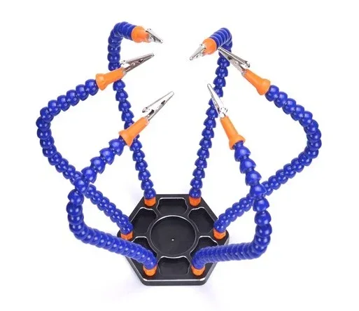
6 Flexible Arms Soldering Station With Swiveling Alligator Clip
Hold your PCB steady while soldering SMD ICs. The flexible arms and alligator clips free both hands for precise soldering work.
QFN / DFN (Quad Flat No-lead)
QFN (Quad Flat No-lead) packages have contact pads on the bottom surface of the package rather than protruding leads. This gives them a very small footprint, excellent thermal characteristics (the exposed pad on the bottom is often connected to the die for direct heat transfer), and good high-frequency performance due to short lead paths.
Common variants: QFN-16, QFN-20, QFN-32, MLF (Micro Lead Frame). The ESP32 module uses a QFN package for the main SoC die.
Challenge: QFN packages are much harder to solder by hand since the pads are underneath the IC. They are best done with solder paste + stencil + reflow oven. Some makers use hot air rework stations with careful solder paste application. Not recommended for complete beginners.
BGA (Ball Grid Array)
BGA packages use an array of solder balls on the bottom of the package for electrical connection. They can accommodate hundreds or even thousands of connections in a small area. Used for high-pin-count devices like CPUs, GPUs, DDR RAM, and complex FPGAs.
BGA is essentially impossible to hand-solder — it requires IR reflow or convection oven, X-ray inspection for quality verification, and specialised rework stations for repair. For Indian hobbyists, BGA is encountered in smartphone repair (reballing) and professional PCB rework, not in DIY project assembly.
SMD Passive Component Size Codes: 0402, 0603, 0805
While primarily used for passive components (resistors, capacitors), these size codes are essential knowledge for PCB designers working with SMD ICs:
| Code | Size (inch) | Size (mm) | Solderability |
|---|---|---|---|
| 2512 | 0.25×0.12″ | 6.3×3.2 mm | Easy (large) |
| 1206 | 0.12×0.06″ | 3.2×1.6 mm | Easy |
| 0805 | 0.08×0.05″ | 2.0×1.25 mm | Moderate — recommended for beginners |
| 0603 | 0.06×0.03″ | 1.6×0.8 mm | Moderate |
| 0402 | 0.04×0.02″ | 1.0×0.5 mm | Difficult — needs fine tweezers + magnification |
| 0201 | 0.02×0.01″ | 0.6×0.3 mm | Very difficult — microscope required |
Choosing the Right Package for Your Project
Prototyping / Learning Stage
Use DIP packages exclusively. Plug into breadboards, use IC sockets, swap chips without soldering. A DIP-8 NE555, DIP-14 LM358, and DIP-28 ATmega328P will serve you well for 90% of beginner and intermediate projects.
Compact Custom PCB Design
Use SOIC-8/16 for op-amps, drivers, and simple logic ICs. Use TQFP or LQFP for microcontrollers. These are still hand-solderable and significantly reduce PCB size compared to DIP.
Production / Miniaturized Boards
Use QFN or BGA for maximum density. Requires reflow soldering infrastructure but produces the most compact boards.

BAKON Soldering Iron Tip 900M-T-I
A fine chisel tip essential for soldering SOIC, SSOP, and QFP SMD IC packages with precision. Fits 900M compatible stations.
Soldering Tips for SMD Packages
Tools You Need for SMD Soldering in India
- Soldering iron: Temperature-controlled station (Hakko 936 clone or BAKON series) — do NOT use a cheap fixed-wattage iron for SMD
- Tip: 0.5–1mm chisel or bevel tip for SOIC; fine cone tip for QFP fine-pitch
- Solder: 0.3–0.5mm diameter 63/37 leaded solder or SAC305 lead-free
- Flux: No-clean rosin flux gel or liquid — essential for SMD drag soldering
- Solder wick: For removing bridges and excess solder
- Tweezers: Fine-tip ESD-safe tweezers (₹80–₹200 in India)
- Magnification: A USB digital microscope (₹500–₹1500) or loupe (₹100–₹300)

0.1MM Copper Soldering Enamelled Repair Reel Wire
Ultra-fine 0.1mm copper wire perfect for SMD rework, jumper wires between tiny pads, and PCB repair work.
Frequently Asked Questions
Q1: Can I convert a SOIC package to DIP for breadboard use?
Yes! SOIC-to-DIP adapter boards are cheap and widely available (₹15–₹50 per piece online). Solder the SOIC IC onto the adapter board, and now it has standard 2.54mm DIP footprint pins that fit a breadboard. This is an excellent way to prototype with SMD-only ICs.
Q2: What does “PDIP” vs “CDIP” mean?
PDIP = Plastic DIP (standard hobbyist package, black plastic). CDIP = Ceramic DIP (white or grey ceramic body). CDIP is used in military-grade and high-reliability applications where extreme temperature ranges and hermetic sealing are required. For Indian hobbyists, you’ll almost always encounter PDIP.
Q3: Why are many new ICs only available in SMD packages?
As ICs become more complex, pin counts increase beyond what DIP can accommodate. Even for lower pin-count devices, semiconductor manufacturers are phasing out DIP to reduce manufacturing costs and meet demand for smaller PCBs. Many modern microcontrollers (STM32, ESP32 bare die), PMICs, and RF chips are SMD-only.
Q4: What is the difference between SOIC and SSOP?
Both are small-outline SMD packages with two rows of gull-wing pins. SOIC has a 1.27mm pin pitch and is easier to solder by hand. SSOP (Shrink SOP) has a 0.65mm pin pitch — half the spacing — and requires more skill and a finer soldering tip. Both are significantly smaller than equivalent DIP packages.
Q5: How do I read an IC package code like LQFP-64?
The code breaks down as: L = Low-profile, Q = Quad (pins on all 4 sides), F = Flat, P = Package, 64 = number of pins. Similarly, TSSOP-28 = T(hin) S(hrink) S(mall) O(utline) P(ackage) with 28 pins. Once you understand the prefix meanings, most IC package codes become self-explanatory.
Get Your PCB Prototyping Supplies at Zbotic
From universal PCB boards and soldering accessories to DIP ICs and jumper wires — everything you need to go from schematic to working circuit, delivered fast across India.


Add comment