
Charge Pump Circuit: Doubler and Inverter Design Tutorial
What if you could generate -5 V from a +5 V supply, or produce 12 V from a single 6 V battery — using nothing but capacitors and diodes? That’s the magic of a charge pump circuit design. No inductors, no transformers, no magnetic cores — just switched capacitors doing the heavy lifting. Charge pumps are everywhere: inside op-amp ICs that need dual supplies, in flash memory programming circuits, in LCD bias generators, and in countless embedded systems where small amounts of charge-pumped voltage are needed without the complexity of an inductor-based converter.
How a Charge Pump Works: The Core Principle
A charge pump exploits the fundamental property of a capacitor: it can transfer electric charge from one voltage level to another. The basic operation involves two phases:
Phase 1 – Charge: A capacitor (called the “flying capacitor” or “pump capacitor”) is connected to the input voltage source and charges up to the input voltage (Vin). Think of it as filling a bucket with water.
Phase 2 – Transfer: The charged capacitor is then disconnected from the input and reconnected in a different configuration — for example, stacked in series with the input supply. The charge it stored adds to (or subtracts from) the input voltage, producing a higher (or lower or inverted) output at the output capacitor.
By repeating this cycle rapidly (typically at 10 kHz to 1 MHz), the charge pump maintains a steady DC output voltage at the new level. The switching is performed by MOSFET switches (in ICs) or diodes (in discrete designs).
The critical limitation: Charge pumps are current-limited. Because each cycle transfers a fixed amount of charge (Q = C × V), the output current depends on switching frequency and capacitor value: I_out = C × V × f. Typical charge pump ICs deliver 10–200 mA. For higher currents, inductor-based boost/buck converters are needed.
Voltage Doubler Circuit: Double Your Supply
The classic Villard voltage doubler uses two diodes and two capacitors to produce 2×Vin from an AC or square wave input. Here’s how the most common half-wave doubler works:
Half-Wave Voltage Doubler (Diode-Capacitor)
Components:
- C1: pump capacitor (e.g., 10 µF)
- C2: output filter capacitor (e.g., 100 µF)
- D1: rectifier diode (1N4007 or Schottky)
- D2: rectifier diode
- Input: square wave from oscillator or PWM (e.g., 10 kHz from Arduino)
Circuit topology:
- Input AC/square wave → C1 in series → output node
- D1: anode to input (before C1), cathode to GND (clamps negative swings)
- D2: anode to junction of C1 and D1 cathode, cathode to output → C2 to GND
Operation:
- When input goes negative: D1 conducts, C1 charges to Vpeak through D1
- When input goes positive: D1 blocks, D2 conducts. Now C1’s charged voltage adds to the input peak, pushing the output to 2×Vpeak
- C2 filters the output to a smooth 2×Vpeak DC level
Practical example with Arduino PWM: Generate a 10 kHz square wave (0–5 V) using a Timer1 PWM at 50% duty cycle. Feed through the doubler circuit. Output: approximately 8–9.5 V DC (2×5 V minus two diode drops of 0.7 V each). Add a 10 kΩ load to test output regulation. The output will sag under load — add more capacitance (100 µF) to improve it.
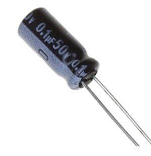
0.1µF 50V Capacitor (Pack of 50)
Capacitors are the heart of every charge pump circuit. These 100 nF 50 V capacitors are perfect for pump and bypass applications in voltage doubler and inverter designs.
Voltage Inverter: Generating Negative Voltage
A charge pump voltage inverter produces a negative voltage equal in magnitude to the input (i.e., from +5 V it produces -5 V). This is invaluable whenever you need a split supply (e.g., ±5 V for an op-amp) but only have a single-rail supply available.
Discrete Inverting Charge Pump
Components:
- C1: pump capacitor (10 µF electrolytic)
- C2: output filter capacitor (100 µF electrolytic)
- D1, D2: Schottky diodes for minimum voltage drop (e.g., 1N5819)
- Oscillator: square wave at Vin amplitude (0 to Vin), 10–100 kHz
Operation:
- Phase 1 (CLK high): D1 conducts, C1 charges to Vin with positive plate at Vin
- Phase 2 (CLK low): D1 blocks, D2 conducts. C1’s positive plate is grounded through CLK, so negative plate falls to -Vin. D2 conducts and charges C2 to -Vin
- Result: steady -Vin at output, referenced to system GND
Using Schottky diodes reduces the voltage drop from 0.7 V per diode to about 0.3 V, giving -4.4 V from +5 V input instead of -3.6 V with silicon diodes. For even less drop, MOSFET-switched charge pumps (used inside ICs) eliminate the diode drop entirely using synchronous rectification.
Output Impedance and Load Regulation
The output impedance of a charge pump inverter is approximately: Z_out ≈ 1/(2 × C × f)
For C=10 µF, f=10 kHz: Z_out ≈ 5 Ω. This means at 10 mA load, you lose 50 mV of output voltage — quite good. Doubling the frequency halves the output impedance.
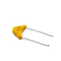
100nF Multilayer Ceramic Capacitor (Pack of 50)
Low-ESR ceramic capacitors improve charge pump efficiency and reduce output ripple. Use these alongside electrolytics for the best output regulation in your inverter design.
Voltage Multiplier (Cockcroft-Walton Ladder)
The Cockcroft-Walton (CW) voltage multiplier is a cascade of diode-capacitor stages that can theoretically produce any integer multiple of the input voltage. First built in 1932 to power early particle accelerators, it’s now used in everything from CRT televisions to camera flash units to Nixie tube power supplies — a popular project among Indian electronics hobbyists.
A CW multiplier with N stages produces approximately 2N × Vpeak output voltage (before load). Each stage consists of two capacitors and two diodes arranged in a ladder.
4-stage CW multiplier from 12 VAC (rectified square wave):
- Input: 12 V peak AC
- Theoretical output: 8 × 12 = 96 V DC
- Practical output (with load): 60–75 V DC
- Suitable for: Nixie tube supply (170 V needed — use 8 stages)
The key limitation: output voltage droops significantly under load because each stage has its own impedance that drops voltage. Higher switching frequency and larger capacitors improve regulation. For precision applications, follow the CW multiplier with a linear regulator.
Safety Note: High-voltage charge pumps can charge capacitors to lethal voltages (>50 V). Always use appropriate safety precautions, discharge capacitors before touching, and use insulated probes. This is especially important if you’re building a Nixie tube power supply (180 V).
Charge Pump ICs: ICL7660, MAX660, TC1044
Building a charge pump from discrete components is excellent for learning, but for production projects, dedicated charge pump ICs offer better performance, smaller footprint, and guaranteed specifications.
| IC | Function | Input Voltage | Max Current |
|---|---|---|---|
| ICL7660 | Voltage inverter | 1.5–10 V | 40 mA |
| MAX660 | Inverter + doubler | 1.5–5.5 V | 100 mA |
| TC1044S | Inverter, wide range | 1.5–12 V | 60 mA |
| LM2776 | Inverter, high freq | 2.0–5.5 V | 200 mA |
Using an ICL7660 to generate -5 V from +5 V is trivially simple: connect a 10 µF capacitor between pins 2 and 4 (pump capacitor), another 10 µF from pin 5 to GND (output filter), and the -5 V appears at pin 5. Total component count: the IC plus two capacitors. This -5 V rail can power the negative supply of a single-supply op-amp rail-to-rail output stage, for example.
Key Design Considerations
1. Switching Frequency
Higher frequency = smaller capacitors needed for the same output current capability, but switching losses increase. Most charge pump ICs use 10 kHz–1 MHz internally. For discrete designs with Arduino PWM, 10–100 kHz is practical.
2. Capacitor Type and ESR
Low ESR capacitors (ceramic MLCC or low-ESR electrolytic) improve charge transfer efficiency and reduce output ripple. For the pump capacitor, use ceramic if possible. For the output filter, a combination of electrolytic (bulk charge storage) and ceramic (high-frequency decoupling) works best.
3. Diode Forward Voltage Drop
Each diode in the charge pump subtracts its Vf from the output. For a doubler with two diodes: Vout = 2×Vin − 2×Vf. Use Schottky diodes (Vf ≈ 0.3 V) instead of silicon (Vf ≈ 0.7 V) to improve efficiency.
4. Output Ripple
Charge pumps produce inherent output ripple at the switching frequency. To minimize it: increase switching frequency, increase output capacitor value, add a small RC filter (e.g., 10 Ω + 100 µF) at the output, or follow the charge pump with an LDO regulator.

0.1µF Ceramic Capacitor (Pack of 50)
Ceramic capacitors with low ESR are ideal for charge pump circuits — use them as pump capacitors and output bypass capacitors for cleaner DC output with less ripple.
Practical Applications for Indian Makers
1. Dual-Rail Op-Amp Supply from Single 9 V Battery
Many audio amplifier and instrumentation amplifier circuits require ±5 V or ±9 V. Use a 9 V battery + ICL7660 (or MAX660) to generate -9 V. Both rails are then available for op-amps like LM358 or TL071. This is the go-to solution for battery-powered audio projects.
2. Negative Voltage Bias for Depletion-Mode MOSFETs
Some RF JFETs and depletion-mode MOSFETs require a negative gate bias voltage. A small charge pump inverter supplying -2 V to -5 V from the positive supply rail handles this elegantly without a second battery or transformer.
3. High-Voltage Supply for OLED/E-Ink Displays
Many OLED and e-ink display drivers (like the SSD1306 or IL3897) have internal charge pumps that generate the 10–20 V needed for the display panel from a 3.3 V supply. Understanding charge pump design helps you debug display issues and design custom power supply circuits for these modules.
4. Flash Memory Programming Voltage
Old EPROM and Flash memory chips require 12 V programming pulses even when powered from 5 V. Internal charge pumps in modern flash controllers handle this automatically — understanding the principle helps when working with legacy EEPROM circuits or microcontroller fuse bit programming.
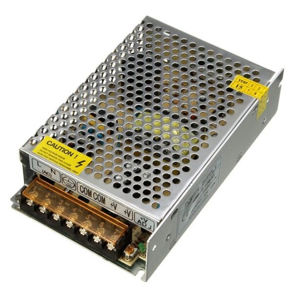
12V 10A SMPS 120W DC Metal Power Supply
A stable 12 V supply is the ideal input for charge pump circuits that need to generate higher voltages. This quality SMPS provides clean DC with low ripple — essential for reliable charge pump operation.
Frequently Asked Questions
Q1: Can a charge pump replace a boost converter?
Only for low-current applications. Charge pumps are limited to ~10–200 mA output due to their capacitive energy storage (no inductor for continuous energy flow). Boost converters can deliver amps of current but are more complex (require inductor, MOSFET, controller IC). Use a charge pump when you need small amounts of voltage-converted power with minimal components.
Q2: Why does my charge pump output voltage drop under load?
This is due to the output impedance of the charge pump: Z_out = 1/(2 × C × f). The output impedance causes a voltage drop proportional to load current. Increase your switching frequency (if using a discrete design) or use a larger pump capacitor. Adding an LDO regulator after the charge pump provides a stable, regulated output regardless of load.
Q3: Can I use the 50 Hz mains AC as the clock for a charge pump?
Technically yes, but 50 Hz is very slow — you’d need very large capacitors (1000 µF or more) to deliver useful current. The resulting ripple at 100 Hz would also be large. Use a higher-frequency oscillator (555 timer, microcontroller PWM) for practical charge pump circuits.
Q4: What is a regulated charge pump?
Some charge pump ICs include a feedback loop that monitors the output voltage and adjusts the switching frequency or duty cycle to maintain a constant output despite load variations. The LTC3201 and MAX232 (the classic RS-232 driver) use regulated charge pumps internally. The output voltage of a regulated charge pump stays stable across a range of loads — unlike an unregulated charge pump which droops under load.
Q5: How do I reduce charge pump noise in audio circuits?
Charge pumps operating at audible frequencies (< 20 kHz) inject switching noise into the supply rail that can appear as a whine in audio circuits. Solutions: increase switching frequency above 100 kHz (outside audio range), add LC filter at output, use a regulated charge pump IC with spread-spectrum modulation, or follow the charge pump with an LDO linear regulator to absorb switching ripple.
Generate Any Voltage You Need
Charge pumps give you the power to create negative voltages, double your supply, and generate custom voltage rails — all from simple capacitors and diodes. Whether you’re powering an op-amp circuit, driving a display, or experimenting with high-voltage Nixie tubes, charge pump circuits open up new possibilities for your projects.


Add comment