
Most analog sensors produce output signals that are too small, offset, or noisy to be directly fed into a microcontroller ADC. A thermocouple generates millivolts. A load cell bridge outputs microvolts. A photodiode produces nanoamperes of current. Without proper signal conditioning, these signals are lost in noise or misread by the ADC. Op-amp circuits are the fundamental building blocks that bridge the gap between raw sensor output and clean, accurate digital data.
This guide covers the key analog sensor signal conditioning op-amp circuit designs that every electronics hobbyist and embedded systems engineer should know — from basic non-inverting amplifiers to differential instrumentation amplifiers and active filters.
Why Signal Conditioning Is Needed
A microcontroller ADC has three fundamental requirements: the input voltage must be within range (e.g., 0–3.3 V), the source impedance must be low enough not to affect the ADC sample-and-hold accuracy, and the signal must be stable enough to read reliably.
Raw sensors routinely violate all three requirements:
- A K-type thermocouple produces 41 µV/°C — a 200°C measurement is only 8.2 mV, far below the ADC range and buried in amplifier noise
- A 350 Ω load cell bridge has a 350 Ω source impedance, which creates ADC errors on successive-approximation converters
- A light-dependent resistor (LDR) changes resistance by 6 decades but needs level shifting to produce a useful voltage swing
Signal conditioning solves all of these problems systematically.
Op-Amp Basics for Sensor Circuits
An ideal operational amplifier has infinite gain, infinite input impedance, zero output impedance, and zero offset voltage. Real op-amps approach these ideals closely enough that the ideal analysis produces accurate designs for most sensor applications.
Golden Rules of Op-Amp Analysis (Negative Feedback)
- The output drives the inverting input to equalise it with the non-inverting input (virtual short)
- No current flows into the op-amp input terminals (virtual open circuit)
Using these two rules, you can derive the transfer function for any op-amp topology without solving differential equations.
Key Non-Ideal Parameters That Matter in Sensor Designs
- Input offset voltage (Vos): DC error at zero differential input. Critical for precision measurements. Rail-to-rail op-amps often have 0.5–5 mV offset. Precision op-amps like the OPA2333 have <25 µV.
- Bias current (IB): Small current drawn by input transistors. Creates voltage error across source impedances. JFET and CMOS op-amps have picoamp bias currents; BJT inputs draw nanoamps to microamps.
- Gain-bandwidth product (GBW): Limits maximum gain at a given frequency. An op-amp with 1 MHz GBW at unity gain has only ×10 gain available at 100 kHz.
- Noise voltage (en): Intrinsic voltage noise, typically expressed as nV/√Hz. At 10 nV/√Hz, a 10 kHz bandwidth produces √(10,000) × 10 nV = 1 µV RMS of noise referred to the input.
Voltage Follower (Buffer)
The voltage follower is the simplest and most universally useful signal conditioning circuit. It has unity gain (Vout = Vin) but transforms the source impedance from potentially hundreds of kilohms down to milliohms.
       +V
        |
        |
 Vin ---+--- (+)
             |   _____ Vout
             | op /(connected back to -)
             |-  /
        |   (-)/
        |
       -V
Use case: Any high-impedance sensor (resistive soil moisture sensor, LDR, thermistor divider) before connecting to a microcontroller ADC. Even a 10 kΩ source impedance can cause measurable errors on a 10-bit ADC with a 1 kΩ sample-and-hold impedance.
Practical Circuit Values
Connect the sensor output to the non-inverting (+) input. Connect the output directly back to the inverting (−) input. That’s it — no resistors needed. Power from a 3.3 V or 5 V single supply (use an LMV321, MCP6001, or TLV2371 for single-supply operation).
Non-Inverting Amplifier
For sensors that produce small voltages (thermistors near mid-scale, analog pressure sensors), the non-inverting amplifier boosts the signal to fill the ADC input range.
Transfer Function
Vout = Vin × (1 + R2/R1)Gain is always ≥ 1. For an LM35 temperature sensor (10 mV/°C) connected to a 3.3 V ADC, measuring 0–100°C (0–1 V range):
Required gain = 3.3 V / 1 V = 3.3x
1 + R2/R1 = 3.3
R2/R1 = 2.3
→ Use R1 = 10 kΩ, R2 = 23 kΩ (use 22 kΩ standard value)
LM35 Temperature Sensors
The LM35’s linear 10 mV/°C output is a classic signal conditioning exercise — amplify its output with a non-inverting stage to span the full ADC range for maximum resolution.
Difference Amplifier
The difference amplifier amplifies the difference between two voltages while rejecting common-mode signals. This is essential for bridge sensors (Wheatstone bridge configurations used in load cells and pressure sensors) where both inputs ride on a large common-mode voltage.
Transfer Function (equal resistors: R1 = R2 = R3 = R4 = R)
Vout = (V+ - V-) × R2/R1Critical limitation: Common-mode rejection ratio (CMRR) is highly sensitive to resistor matching. A 0.1% resistor mismatch limits CMRR to approximately 66 dB. For higher CMRR, use a precision resistor network (quad-matched package) or switch to an instrumentation amplifier.
Instrumentation Amplifier (INA)
The instrumentation amplifier is the gold standard for sensor signal conditioning. It provides very high input impedance on both inputs, excellent CMRR (typically 80–110 dB), programmable gain set by a single external resistor, and is available in single-package ICs.
Popular INA ICs for Sensor Applications
| IC | Gain Range | CMRR (dB) | Vos (µV typ) | Best For |
|---|---|---|---|---|
| INA128 | 1–10,000 | 120 | 50 | General purpose |
| INA333 | 1–1,000 | 100 | 25 | Low-power 3.3 V systems |
| AD8221 | 1–1,000 | 110 | 60 | Medical / precision |
| INA219 | Fixed internal | 80 | — | Current sensing (I2C output) |
INA128 Gain Setting Formula
G = 1 + (50 kΩ / Rg)

For G = 100: Rg = 50,000 / (100 - 1) = 505.05 Ω → use 499 Ω (1%)
For G = 500: Rg = 50,000 / 499 = 100.2 Ω → use 100 Ω (1%)
The INA128 is the standard choice for load cell signal conditioning. A 1 kg load cell with 2 mV/V excitation at 5 V produces 10 mV full-scale. With G = 300 (Rg = 168 Ω), the output spans 3 V — well within the ADC range.
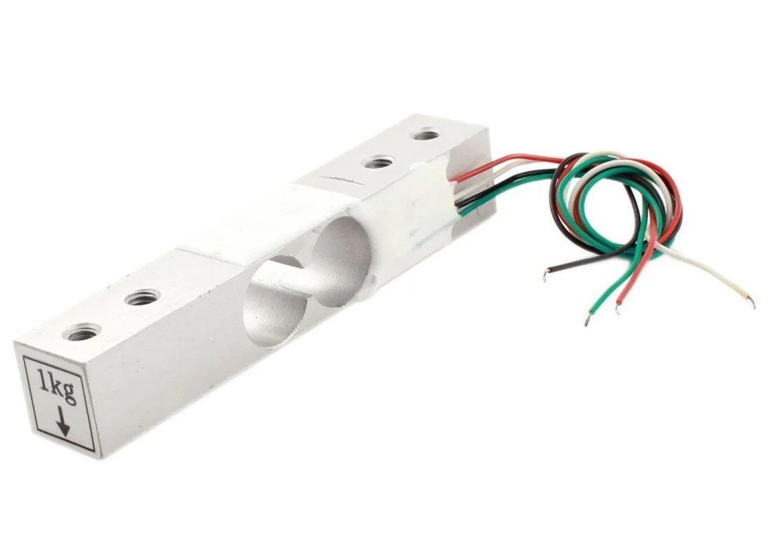
1Kg Load Cell – Electronic Weighing Scale Sensor
A Wheatstone bridge load cell is the perfect application for an instrumentation amplifier — the INA128 with a precision Rg resistor gives you clean, amplified weight data.
Offset Correction Circuit
Many sensors have a non-zero output at the zero-stimulus condition (zero pressure, zero temperature, zero force). To maximise ADC resolution, this offset must be subtracted before amplification.
Method 1: Resistor Summing Network
A summing amplifier adds a precise negative DC offset to cancel the sensor’s idle voltage. Using a precision voltage reference (TL431, LM4040) ensures the offset is stable across temperature.
Method 2: Digital Offset via ADC Reference
If the offset is small relative to the ADC range, subtract it in firmware: read the sensor at zero stimulus, store as baseline, subtract from all subsequent readings. Simple but sacrifices ADC resolution proportional to the offset magnitude.
Method 3: Trim Potentiometer
A 10 kΩ trim potentiometer on the reference input of a difference amplifier provides adjustable offset nulling. Use a multiturn cermet trimmer for stable, drift-free setting in production designs.
Active Low-Pass Filter (Sallen-Key)
Sensor signals are often contaminated with high-frequency noise: 50 Hz mains hum, switching regulator ripple, RF interference, and mechanical vibration. A passive RC filter works but loads the source and rolls off gradually. An active Sallen-Key filter provides a sharper response with zero loading effect.
Sallen-Key 2nd-Order Low-Pass Filter
For a cutoff frequency fc with Butterworth (maximally flat) response, use equal-value resistors (R) and capacitors (C) related by:
fc = 1 / (2π × R × C × √2)

For fc = 100 Hz:
Choose C = 100 nF
R = 1 / (2π × 100 × 100e-9 × 1.414)
  = 11,254 Ω → use 11 kΩ or 10 kΩ + 1 kΩ trimmer
The Sallen-Key configuration uses a standard voltage follower (or low-gain non-inverting amplifier) with the RC network in the feedback path. Two identical RC stages provide 40 dB/decade attenuation above cutoff — sufficient to attenuate 1 kHz switching noise to 1% of its amplitude when the cutoff is set at 100 Hz.
Anti-Aliasing Filter
When sampling with an ADC at rate fs, signals above fs/2 (the Nyquist frequency) fold back (alias) into the baseband and cannot be distinguished from real signals. An anti-aliasing filter must attenuate everything above fs/2 to below the ADC noise floor before sampling. For a 1 kHz sampling rate, set the anti-aliasing cutoff at 400–450 Hz.
Transimpedance Amplifier (TIA) for Photodiodes
Photodiodes generate a current proportional to light intensity (typically nanoamperes to microamperes). A transimpedance amplifier converts this current to a voltage.
Vout = -Iph × Rf

For Iph = 1 µA at full scale, targeting 1 V output:
Rf = 1 V / 1 µA = 1 MΩ
At high values of Rf, the op-amp’s bias current error becomes significant. Use a JFET-input or CMOS op-amp (LF356, TLC2272, OPA2134) with picoamp bias currents when using feedback resistors above 100 kΩ.
Stability: Large feedback resistors combined with input capacitance (from the PCB and photodiode junction) can cause oscillation. Add a small feedback capacitor (1–10 pF) in parallel with Rf to stabilise the circuit.
Current-to-Voltage Converter (4–20 mA Loop)
The 4–20 mA current loop is the standard industrial sensor interface for long-cable-run environments. The sensor transmits a current between 4 mA (zero scale) and 20 mA (full scale) regardless of cable resistance (up to hundreds of ohms).
Passive Conversion: Shunt Resistor
Vout = I × Rshunt

For 4–20 mA to 0.8–4 V (for a 5 V ADC):
Rshunt = 0.8 V / 4 mA = 200 Ω

Range check: 20 mA × 200 Ω = 4 V ✓ (within 5 V range)
A 200 Ω resistor (or 180 Ω + 22 Ω in series) placed in the return wire converts the 4–20 mA loop to 0.8–4 V. Follow with a voltage follower before the ADC to provide impedance isolation. In firmware, map: 0.8 V → 0%, 4.0 V → 100%.
Op-Amp Selection for Sensor Applications
| Application | Priority | Recommended ICs |
|---|---|---|
| Single-supply 3.3 V, general | Rail-to-rail I/O, low cost | LMV321, MCP6001 |
| Precision DC measurement | Low Vos, low drift | OPA2333, LTC2050 |
| High-impedance source (LDR, pH) | Low bias current (JFET/CMOS) | LF356, TL071, OPA134 |
| Photodiode / TIA | Low noise, JFET input | OPA2134, LF356 |
| Audio-frequency filtering | Low noise, wide bandwidth | NE5532, OPA1642 |
| Battery-powered sensors | Micropower | LPV811, MAX44246 |
PCB Layout for Low-Noise Op-Amp Circuits
Guard Ring Technique
For high-impedance inputs (pH electrodes, electrometer circuits), leakage current across the PCB surface can exceed the sensor current. A guard ring — a copper trace surrounding the input pin, connected to the output of the voltage follower — drives the PCB surface to the same potential as the input, eliminating leakage current paths. This is essential for source impedances above 10 MΩ.
Separate Analog and Digital Grounds
Run analog signal ground and digital ground as separate copper pours on the PCB. Connect them at a single point near the power supply decoupling capacitors. This prevents digital switching currents from flowing through the analog ground plane and creating noise voltages at the op-amp inputs.
Component Placement
Place feedback resistors as close as possible to the op-amp pins to minimise parasitic capacitance. Avoid routing high-speed digital traces near op-amp inputs. Use 0402 or 0603 resistors for signal path components — larger packages add more parasitic capacitance.
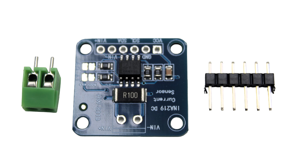
INA219 I2C Bi-directional Current/Power Monitor
The INA219 integrates a precision difference amplifier and 12-bit ADC in one chip — a ready-made signal conditioning solution for current measurement up to 3.2 A.
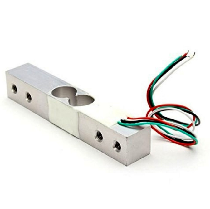
10Kg Load Cell – Electronic Weighing Scale Sensor
A 10 kg strain gauge load cell is the ultimate test for instrumentation amplifier design — its µV-level bridge output demands precise signal conditioning.
Frequently Asked Questions
Q: Can I use a single-supply op-amp for a signal that swings around 0 V?
A: Only if the op-amp is specifically rated for rail-to-rail input down to 0 V (marked RRIO — rail-to-rail input and output). Standard op-amps on a single 5 V supply cannot amplify signals below approximately 1–2 V above the negative rail. For bipolar signals, use a dual-supply (±5 V) or add a virtual ground at Vcc/2 and AC-couple the signal.
Q: My op-amp output is clipping at the positive rail. What is wrong?
A: Either the gain is too high, the input voltage is too high, or the offset is pushing the output into saturation. Calculate the maximum expected input × gain and ensure the result is at least 0.5 V below the positive supply (for non-rail-to-rail op-amps, 1.5–2 V headroom is needed).
Q: What is the difference between an instrumentation amplifier and a differential amplifier?
A: A differential amplifier uses four resistors and one op-amp. Its input impedance is limited by the resistor values (typically 10–100 kΩ) and CMRR degrades with resistor mismatch. An instrumentation amplifier uses three op-amps internally, providing extremely high input impedance (GΩ) on both inputs, gain set by a single resistor, and CMRR of 80–120 dB regardless of gain setting.
Q: How do I eliminate 50 Hz hum from my sensor readings?
A: Several approaches work together: (1) use a low-pass filter with cutoff below 50 Hz for DC or slowly changing signals, (2) integrate the ADC reading over exactly 20 ms (one 50 Hz cycle) — this cancels the 50 Hz component, (3) shield signal cables with grounded screen, (4) use twisted-pair wiring for differential sensor connections, (5) avoid routing signal wires near mains transformers or power cables.
Q: Is it better to use an external op-amp or rely on the Arduino’s built-in ADC?
A: The Arduino’s ATmega328 ADC is 10-bit with ±2 LSB accuracy and 100 kΩ effective input impedance. For many sensor applications this is adequate with only a voltage follower buffer. For precision measurements (weight, thermocouple temperature, strain), an external instrumentation amplifier plus a 24-bit delta-sigma ADC (HX711 for load cells, ADS1115 for general purpose) dramatically outperforms the built-in ADC at low cost.
Q: Why does my signal conditioning circuit work fine on the bench but add noise in the field?
A: Field environments have higher EMI (motors, variable frequency drives, RF transmitters). Best practices for field-robust circuits: use ferrite beads on power supply pins, add 100 nF ceramic decoupling directly at op-amp supply pins, use metal enclosures, shield signal cables, add ESD protection diodes on all inputs, and use differential (instrumentation amplifier) topology to reject common-mode interference on long cable runs.
Conclusion
Signal conditioning is the bridge between raw sensor physics and clean digital data. Mastering the voltage follower, non-inverting amplifier, instrumentation amplifier, and active filter gives you the tools to handle virtually any analog sensor interface challenge — from millivolt thermocouple outputs to picoamp photodiode currents.
The key design decisions are straightforward: select the topology based on the source impedance and signal amplitude, choose an op-amp whose offset voltage and bias current are insignificant relative to your accuracy requirement, apply the three-tier decoupling on the power supply, and lay out the PCB with a solid analog ground plane.
Explore Zbotic’s complete range of sensors and measurement modules — all compatible with the signal conditioning circuits described in this guide.
Explore Sensors & Measurement Modules
Find sensors, INA modules, load cells, and measurement tools at Zbotic — shipped fast across India.


Add comment