
Every electronics project eventually hits the same wall: sensitive circuits misbehaving because the power supply is noisy. Microcontrollers resetting, op-amp outputs oscillating, ADC readings jumping erratically, RF modules dropping connections — these are all classic symptoms of power supply ripple and noise. Understanding and applying effective ripple noise reduction techniques in power supply design is one of the most valuable skills any Indian electronics hobbyist or engineer can develop. This comprehensive tutorial covers everything from fundamentals to practical PCB layout techniques.
What Causes Power Supply Ripple and Noise?
Ripple and noise in power supplies come from distinctly different sources, and treating them effectively requires understanding each one:
Ripple (Low Frequency, 50-120 Hz and Switching Frequency)
Ripple is the periodic variation in DC output voltage that follows the frequency of the power source. In a linear power supply using a transformer and rectifier from India’s 50Hz mains, the output will have ripple at 100Hz (for full-wave rectification). In a switch-mode power supply (SMPS), ripple appears at the switching frequency, typically 50kHz-2MHz. Ripple amplitude is primarily determined by the output capacitor value and the load current demand.
Noise (High Frequency, MHz Range)
High-frequency noise is generated by the fast switching edges of MOSFETs and diodes in SMPS designs. Each switching transition (nanoseconds fast) radiates both conducted and radiated EMI. This noise couples through parasitic capacitances and inductances on the PCB, appearing on the output rail as random spikes and hash that standard oscilloscope measurements may underestimate (most oscilloscopes have limited bandwidth probes).
Load Transients
When a load suddenly draws more current (a motor starting, a Wi-Fi module transmitting), the power supply output voltage dips momentarily before the control loop compensates. This transient ripple is separate from the steady-state ripple and is reduced by increasing output capacitance and improving the supply’s load transient response (higher bandwidth control loop).
Ground Bounce
In digital circuits, simultaneous switching of multiple outputs drives transient currents through the PCB’s ground plane. If the ground has significant inductance (thin traces, shared return paths), this creates voltage differences between different parts of the ground plane — effectively adding noise to everything referenced to it.
Measuring Ripple: What Numbers Matter
Before you can reduce ripple, you need to measure it accurately. Several important caveats for makers:
- Oscilloscope probe tip length matters: Use the shortest possible ground lead on your oscilloscope probe. A 10cm ground lead forms an LC loop that resonates in the MHz range and can show phantom noise that doesn’t exist. Ideal: use a proper SMA or SMB connector on the PCB for measurements.
- AC coupling: Set your oscilloscope to AC coupling to remove the DC offset and zoom into the ripple detail. Set vertical scale to 20-50mV/div for typical SMPS ripple.
- Bandwidth limiting: Most oscilloscopes have a 20MHz bandwidth limit switch. For measuring switching ripple at 100-500kHz, leave full bandwidth on. For measuring only 100Hz mains ripple, 20MHz limiting can reduce high-frequency noise in your measurement (not in your circuit).
- Specify ripple as peak-to-peak (Vpp): Not RMS. Vpp tells you the worst-case swing the circuit must tolerate. Typical specs: linear LDO output less than 1mVpp, quality SMPS output less than 20mVpp, standard SMPS output 50-100mVpp.
Bulk and Decoupling Capacitors: The First Defence
Capacitors are the most fundamental ripple reduction tool. Their function varies by capacitance value and placement:
Bulk Capacitors (100uF – 10,000uF, Electrolytic)
These are the large electrolytic capacitors near the power input of a board or module. They provide energy during load transients and reduce low-frequency (50-1000Hz) ripple. The required value is approximately:
C = (Delta-I x Delta-T) / Delta-V
Where Delta-I = load current step, Delta-T = supply response time, Delta-V = maximum allowable voltage droop
For a 1A transient load step, 1ms response time, and 50mV maximum droop: C = (1 x 0.001) / 0.05 = 20uF. In practice, use 100uF to 470uF to account for capacitor ESR and aging. For mains-rectified supplies, the standard rule of thumb is 1000-2000uF per ampere of output current for plus-or-minus 1V ripple at 50Hz.
Key selection criteria: Choose low-ESR (Equivalent Series Resistance) electrolytics rated for 105 degrees C, especially in India where ambient temperatures are high. Standard 85 degrees C capacitors fail much faster under thermal stress. Panasonic FM, Nichicon PW, or Rubycon ZL series are reliable choices available from quality component suppliers.
Ceramic Bypass Capacitors (100nF – 10uF, X5R/X7R)
Place a 100nF ceramic capacitor at every IC power pin, as close to the pin as physically possible. These low-ESR, low-inductance capacitors handle high-frequency transients (10MHz+) that bulk electrolytics cannot respond to due to their inductance. Use X7R or X5R dielectric — not Y5V or Z5U, which lose more than 80% of their capacitance under DC bias and temperature variation.
For modern high-speed ICs (ESP32, Raspberry Pi, STM32), add a 10uF X5R ceramic in parallel with the 100nF. This combination provides low impedance from 100kHz to 100MHz.
The Impedance Profile Trick
Plot the parallel combination of your capacitors’ impedance vs frequency. You want the power supply impedance to be flat and low (below 10 milliohms ideally) from DC to the highest frequency your circuit switches at. Each capacitor type covers a different frequency range — their parallel combination can achieve this if sized correctly.
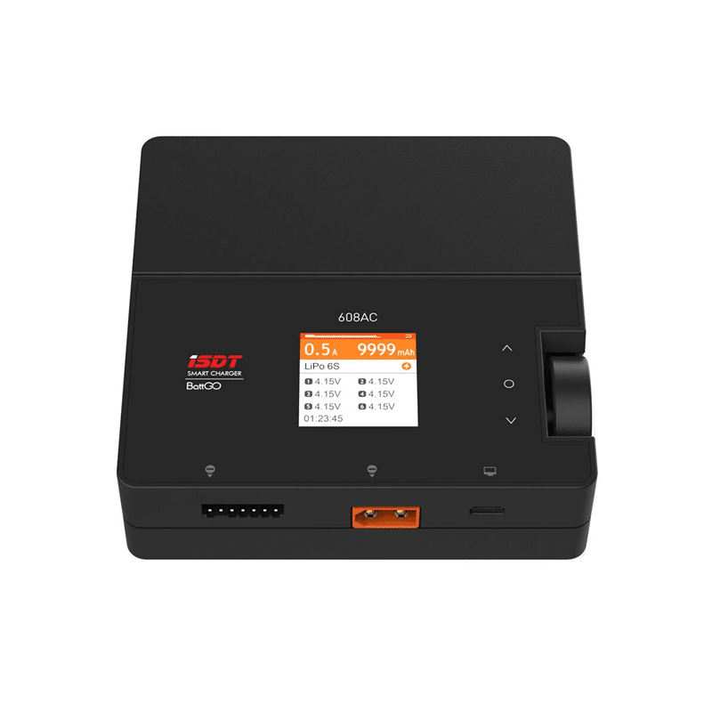
ISDT 608 AC LiPo Battery Charger – AC 50W / DC 200W Dual Mode
A professional-grade AC/DC lab charger with internal SMPS and low-ripple output. An excellent benchmark for low-noise power supply design — study its output ripple characteristics as a reference when designing your own power stages.
Ferrite Beads and Inductors for High-Frequency Noise
Ferrite Beads
A ferrite bead is essentially a lossy inductor — it presents increasing impedance as frequency rises, but instead of storing energy (like a real inductor), it dissipates it as heat. This makes it ideal for filtering high-frequency noise without causing resonance peaks that traditional LC filters can produce.
Connection: Place the ferrite bead in series on the power supply line, with a capacitor to ground after it (a pi or L filter topology). Choose a bead with impedance of at least 100 ohms at your target noise frequency (e.g., 100 ohms at 100MHz for typical digital switching noise). Critically, the bead’s rated current must exceed your load’s maximum current — underrating causes saturation, turning the bead into a plain wire at high current.
Example: For filtering an ESP32’s 3.3V supply rail from a noisy buck converter, place a 600 ohm at 100MHz ferrite bead (rated 2A) in series, then add 10uF + 100nF ceramics to ground after the bead. This will reduce noise above 10MHz by 20-40dB.
Power Inductors in LC Filters
For more aggressive low-frequency ripple reduction, an inductor-capacitor (LC) filter after the SMPS output works well. A 10uH power inductor with 470uF + 10uF capacitors forms an LC filter with a cutoff frequency of about 5kHz, reducing ripple at the 100kHz switching frequency by 26dB or more. Use a shielded, low-DCR inductor to avoid additional losses.
LDO Post-Regulation for Ultra-Low Noise
For the most noise-sensitive loads — precision ADCs, audio circuits, RF front ends, PLL circuits — no amount of passive filtering is as effective as an LDO (Low-Dropout) linear voltage regulator placed after the SMPS output.
An LDO acts as an active noise filter. Its power supply rejection ratio (PSRR) — the ability to reject noise on its input from appearing on its output — is typically 60-80dB at low frequencies, dropping to 20-40dB at 1MHz and nearly 0dB at 10MHz+. Choose LDOs specifically for their PSRR bandwidth: LT3045, ADP7142, or LP5907 all have PSRR greater than 60dB up to 1MHz, making them excellent for post-regulating a 5V SMPS output down to 3.3V for sensitive analog circuits.
The technique is called a hybrid supply: SMPS for efficiency and bulk energy delivery, LDO for the final clean supply rail. The SMPS output can be 5-10% above the final required voltage (e.g., 3.6V output for an LDO targeting 3.3V), minimising the LDO’s power dissipation while achieving the noise performance of a linear supply.
LDO Output Noise Optimisation
- Add a 1uF to 10uF capacitor on the LDO’s noise bypass pin (if present — pins like NC, BYPASS, or NR) to reduce broadband output noise by 10-20dB.
- Use the LDO manufacturer’s recommended output capacitor type and value — some LDOs are unstable with certain capacitor ESR values. Check the datasheet carefully.
- Route the LDO output to sensitive loads on a separate copper plane section with only a single connection to the noisy digital ground via a thin trace (star grounding).
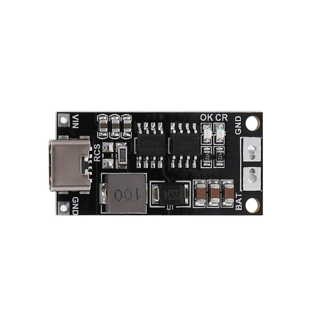
18650 Type-C to 3S 12.6V 2A Booster Module
A compact boost converter that converts 18650 cell voltage to 12.6V output. Use it as a study subject for SMPS ripple reduction: add bulk capacitors and ferrite bead filters to its output while measuring ripple improvement with an oscilloscope.
PCB Layout Techniques That Make or Break the Design
The best schematic design can be ruined by poor PCB layout. Conversely, careful layout can make a mediocre design work surprisingly well. For power supply noise specifically, these layout rules are non-negotiable:
Rule 1: Minimise High-Current Loop Areas
Every high-frequency current loop in your SMPS (the loop formed by the switch, diode, and output capacitor) radiates EMI proportional to the area of that loop. Route these components to minimise the enclosed area — place them as physically close together as possible with short, direct copper paths. In a buck converter, the critical loop is: input capacitor to MOSFET to inductor to output capacitor to ground and back to input capacitor.
Rule 2: Solid Ground Plane
Use a continuous ground plane on at least one PCB layer. Avoid slits, cuts, or long traces across the ground plane in the return path of any high-current switching circuit. A slotted ground plane forces return currents to take longer paths, increasing inductance and radiating EMI. The single most impactful layout improvement you can make to any power supply PCB is adding a solid ground plane.
Rule 3: Decoupling Capacitor Placement
Place 100nF bypass capacitors on the PCB before routing them in the schematic, then route power through the capacitor to the IC pin. The capacitor must be on the same side of the PCB as the IC, as close as physically possible (under 1-2mm from the power pin if using SMD components). The via connecting the capacitor to the ground plane should be adjacent to the capacitor’s ground pad, not across the board.
Rule 4: Separate Analog and Digital Ground Planes
For mixed-signal designs, keep the digital and analog portions of the PCB physically separated. Connect the two ground planes at a single point — typically at the power supply’s output capacitor or at the main filter stage. This prevents digital switching currents from flowing through the analog ground plane and injecting noise into sensitive analog signals.
Rule 5: Inductor Orientation
Unshielded inductors (common on many cheap DC-DC modules) radiate a magnetic field that couples into nearby signal traces. Rotate the inductor 90 degrees if possible to change the coupling direction. Better: always use shielded inductors in noise-sensitive designs — the extra cost is trivial compared to hours of debugging EMI issues.
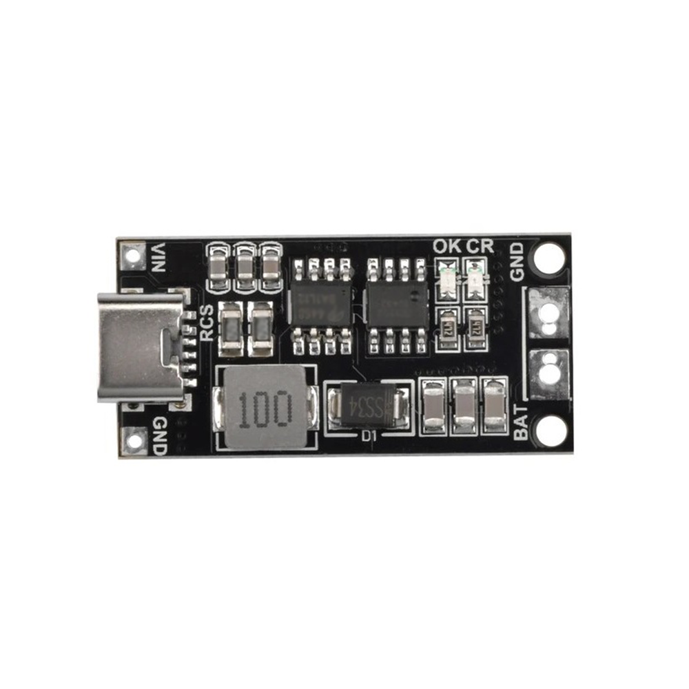
18650 Type-C to 3S 12.6V 4A Booster Module
A higher-current 4A boost module from 18650 to 12.6V. At 4A output, ripple and noise management becomes more critical — an excellent practical platform to apply the filtering techniques described in this guide with real, measurable results.
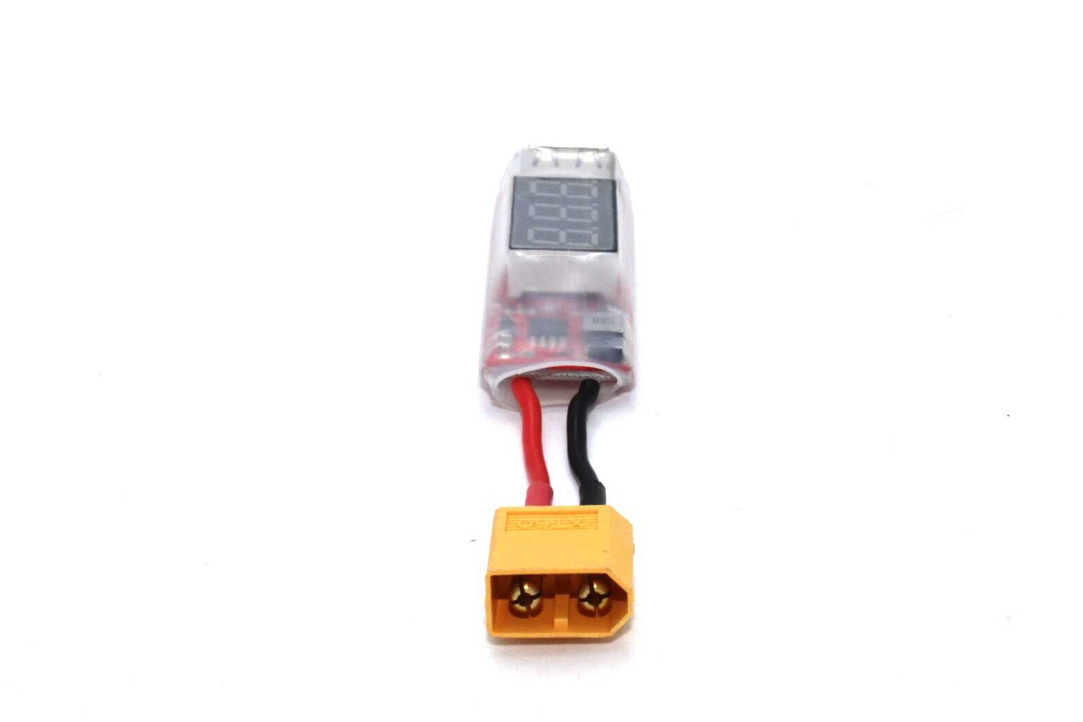
2S-6S LiPo XT60 to USB Adapter with Voltage Display
A multi-cell LiPo to USB adapter with internal switching regulator. Useful as a portable DC lab supply for noise measurement experiments — its internal SMPS output ripple can be directly measured and improved with external filtering as a hands-on learning exercise.
Frequently Asked Questions
My Arduino resets randomly — could it be power supply noise?
Yes, absolutely. Random resets on Arduino boards, especially when motors or relays switch, are a classic symptom of power supply voltage dips (load transients) or noise spikes on the reset pin. Add a 100uF electrolytic + 100nF ceramic across the Arduino’s Vin or 5V pin. Also add a 100nF capacitor from the RESET pin to GND (if not already present on your board) to filter noise spikes. If using a motor driver, power the Arduino from a separate supply or through a ferrite bead + capacitor filter.
What is the difference between ripple and noise in a power supply specification?
Ripple is the periodic, deterministic variation at the switching or mains frequency (predictable, measurable with FFT). Noise refers to broadband, random high-frequency voltage fluctuations. Datasheets often specify output ripple and noise as a combined Vpp figure measured with a 20MHz bandwidth oscilloscope. The bandwidth limit removes very high-frequency components but is a useful standard for comparison between different supplies.
Is a linear power supply always quieter than a switching supply?
In the 10Hz to 1MHz range, yes — a properly designed linear supply is quieter than most SMPS designs. However, a well-designed SMPS with proper filtering can match or exceed a cheap linear supply’s performance. Above 1MHz, the linear supply’s transformer and rectifier can actually radiate more noise than a well-filtered SMPS. For very high precision applications (audio DACs, precision instrumentation), custom low-noise linear supplies are still preferred.
How do I choose between a ferrite bead and an inductor for power line filtering?
Use a ferrite bead when you want to dissipate high-frequency noise without causing resonance (it’s lossy). Use an inductor when you need an LC filter to reduce ripple at a specific frequency (the LC resonance point will depend on your capacitor choice). For digital power rails with unpredictable load steps, ferrite beads are usually preferred to avoid the resonance peaks that LC filters can create if not properly damped.
Does decoupling capacitor distance really matter that much?
Enormously. At 100MHz, a 5mm PCB trace has approximately 3.5nH of inductance, which presents 2.2 ohms of impedance — enough to make a 100nF capacitor ineffective. The difference between a decoupling capacitor at 0.5mm from the IC pin vs 5mm can be 10-20dB at 100MHz. This is not theoretical — it’s measurable with a vector network analyser. Always place decoupling capacitors as close as physically possible to the IC power pin.
Clean Power is the Foundation of Reliable Electronics
Power supply noise is one of the leading causes of mysterious and intermittent failures in electronics projects. The good news is that with the right combination of capacitor selection, ferrite bead filtering, LDO post-regulation, and PCB layout discipline, achieving clean, stable power rails is entirely within reach for any maker. Start with the basics — solid ground planes and proper decoupling — and work up to more advanced techniques as your project demands.
Find all the battery modules, boost converters, and power management components you need to experiment with in Zbotic’s Batteries and Power category. Clean power builds reliable projects.


Add comment