
The current mirror circuit is one of the most elegant and fundamental building blocks in analog electronics. From bias networks in op-amps to reference current sources in ADCs and audio amplifiers, current mirrors appear in virtually every analog IC ever designed. Yet many electronics students in India encounter this topic only in theory, never understanding how to actually build and use one. This practical tutorial walks through the current mirror from first principles to hands-on circuit variants, with calculations you can replicate on your bench today.
What Is a Current Mirror?
A current mirror is a two-port circuit that copies (mirrors) a reference current from one branch into one or more output branches, with high accuracy and independent of the load voltage. Once you set a reference current, every mirror output replicates that same current regardless of what load is connected — as long as the output transistor remains in its active region.
The fundamental principle exploits the matched characteristics of transistors. When two identical transistors share the same base-emitter voltage (VBE for BJTs) or gate-source voltage (VGS for MOSFETs), they pass the same collector/drain current — provided they have the same geometry. Modern ICs fabricate hundreds of matched transistors on the same silicon die, making current mirrors extraordinarily accurate (within 0.1% matching).
Why are current mirrors so important?
- Bias networks: Set the operating point of amplifier stages without resistors (which would require large silicon area)
- Active loads: Replace resistors in differential pairs to dramatically increase gain
- Current references: Generate a stable, temperature-compensated reference current for DACs and ADCs
- Current scaling: Output current = N × Iref using transistor sizing (N output transistors in parallel)
Basic BJT Current Mirror Circuit
The simplest current mirror uses two matched NPN transistors (Q1 and Q2):
VCC ──────────────────────────────────────
        │                    │
       Rref                  RL (Load)
        │                    │
        ├── Q1 Collector      Q2 Collector ──── Iout
        │   Q1 Base ─────────Q2 Base
        │   Q1 Emitter       Q2 Emitter
        │                       /
       Iref        ────────────
                        │
                       GND
More clearly:
- Q1 is the reference transistor (also called the diode-connected transistor). Its collector is tied to its base, forcing it into a configuration that acts like a diode. A reference current Iref flows through it, set by Rref.
- Q2 is the mirror transistor (output transistor). Its base is connected to Q1’s base. Since both transistors have the same VBE (shared base-emitter connection), they pass equal collector currents — so Iout ≈ Iref.
- Rref sets the reference current: Iref = (VCC – VBE) / Rref ≈ (VCC – 0.7V) / Rref
The beauty of this circuit is that Iout is nearly constant regardless of what voltage appears across Q2’s collector (i.e., regardless of RL). This is the hallmark of a current source — it forces the set current into whatever load is connected.
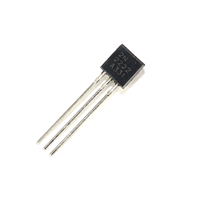
2N2222 NPN Transistor (Pack of 20)
Build basic current mirror circuits with these matched 2N2222 NPN transistors. Select pairs with similar hFE values for best current matching accuracy.
Current Mirror Calculations and Design
Let us design a practical current mirror for 1mA output current from a 12V supply.
Step 1: Choose the Reference Current
Set Iref = Iout = 1mA (for a 1:1 mirror). We want Iref to flow through Rref from VCC.
Step 2: Calculate Rref
Rref = (VCC – VBE) / Iref = (12 – 0.7) / 0.001 = 11.3V / 1mA = 11.3 kΩ
Use the nearest standard value: 11kΩ (giving Iref = 1.027mA). The 10kΩ in E12 series gives 1.13mA — acceptable for most applications.
Step 3: Transistor Selection
For a 1mA current mirror, almost any small-signal NPN transistor works. Key requirements:
- VCEO ≥ VCC (12V in this example) — most small-signal transistors are rated 25V–40V minimum
- IC_max ≥ Iout with safety margin (e.g. BC547 handles 100mA, easily handles 1mA)
- High hFE (current gain) — reduces base current error (see limitations section)
- Matched VBE — select from same batch, or use dual transistors like BC847BS (dual NPN in one SOT-363 package)
Step 4: Verify Operating Region
The output transistor Q2 must remain in the active (forward active) region. This requires VCE(Q2) ≥ VCE_sat (~0.2V typical). As long as your load does not pull the output below about 0.2V, the mirror works correctly. If VCE(Q2) drops below this, Q2 saturates and Iout drops sharply.
Limitations: Base Current Error and Early Effect
The basic two-transistor current mirror has two important sources of error:
1. Base Current Error
Each transistor requires a small base current IB = IC/hFE. In the basic mirror, both Q1 and Q2 base currents are supplied by the reference node. This means the actual reference current flowing through Rref = Iref_actual + 2×IB. The output current error is:
For hFE = 100 (typical for BC547): Iout/Iref = 1/(1 + 0.02) = 0.98 → 2% error. For hFE = 200: ~1% error. For low-gain transistors (hFE = 20), error can reach 10%+ — significant in precision circuits.
2. Early Effect (Channel Length Modulation)
In the basic mirror, Q1’s VCE is fixed at VBE (~0.7V, diode-connected). Q2’s VCE can be anywhere from 0.2V to VCC. Because transistor IC increases slightly with VCE (the Early effect), Iout ≠ Iref when Q2 has a different VCE than Q1. The output current has a slight positive slope with output voltage — this is the finite output impedance of the mirror. High Early voltage transistors (like BC547, VA ≈ 40V) have less error than low Early voltage types.
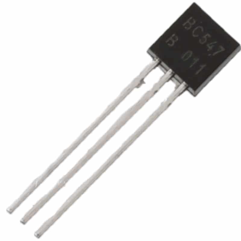
BC547 NPN Transistor TO-92 (Pack of 10)
High hFE (200–800 typical) NPN transistor ideal for current mirror circuits. The high gain minimises base current error, and its 45V VCEO handles 12V supply designs safely.
Wilson and Widlar Current Mirror Variants
Wilson Current Mirror
The Wilson mirror uses three transistors to reduce base current error by two orders of magnitude. A third transistor Q3 is added in the collector of Q1, whose collector supplies the base currents of Q1 and Q2. This feedback arrangement forces the base currents to be self-cancelling, reducing the output error from 2/hFE to approximately 2/hFE².
For hFE = 100: Wilson error ≈ 0.02% vs basic mirror’s 2%. The Wilson mirror also has higher output impedance (better current source behavior), making it preferred for precision bias networks in op-amp input stages.
Widlar Current Mirror
The Widlar mirror (invented by Bob Widlar, the same engineer behind many legendary analog ICs) adds an emitter degeneration resistor to Q2. This enables very small output currents (microamperes) from a moderate reference current (milliamperes) without needing extremely large Rref values. The Widlar mirror is the circuit behind the internal bias currents in most classic op-amps including the LM741 and LM324.
Output current of Widlar mirror:
Iout ≈ VT × ln(Iref/Iout) / RE2
Where VT = 26mV at room temperature, RE2 is the emitter resistor of Q2. Solving this transcendental equation iteratively gives Iout for a chosen RE2. Example: Iref = 1mA, RE2 = 1kΩ → Iout ≈ 10µA.
MOSFET Current Mirror Circuit
MOSFET current mirrors use N-channel or P-channel MOSFETs instead of BJTs. The principle is identical — two MOSFETs sharing the same VGS will carry the same drain current:
VDD ─────────────────────────────────────
     │                       │
    Rref                    Load
     │                       │
     ├── M1 Drain         M2 Drain ──── Iout
     │   M1 Gate ─────── M2 Gate
     │   M1 Source       M2 Source
     │                      /
    Iref        ─────────────
                      │
                     GND
M1 is diode-connected (gate shorted to drain). MOSFET current mirrors have the advantage of theoretically zero gate current error (MOSFETs are voltage-controlled, not current-controlled), so the base current error that plagues BJT mirrors does not apply. However, MOSFETs have larger threshold voltage variations (VTH mismatch), which is the dominant error source in MOSFET mirrors.
MOSFET mirrors are the preferred topology in modern CMOS analog ICs because they scale beautifully — you can create mirrors with output/reference current ratios of 1:100 or 100:1 simply by adjusting transistor width-to-length ratios (W/L). A transistor with W/L = 10 passes 10× the current of one with W/L = 1 at the same VGS.
Practical Applications in Real Circuits
1. LED Current Source
Set a precise current through an LED using a current mirror. Unlike a simple resistor (whose current changes with supply voltage and LED VF variation), a current mirror maintains exactly the set current regardless of supply fluctuations — making LED brightness consistent.
Circuit: Rref sets 20mA reference through Q1. Q2 mirror output drives the LED at exactly 20mA, compensated against supply voltage changes of ±20%.
2. Differential Amplifier Tail Current Source
Every BJT and MOSFET differential pair needs a constant tail current source for its operation. A current mirror (typically a Widlar or Wilson) provides this stable tail current. The tail current directly sets the transconductance and common-mode rejection ratio of the differential amplifier.
3. Active Load in Amplifier Stages
Replacing a resistor load in a common-emitter amplifier with a current mirror active load dramatically increases voltage gain. A resistor’s incremental resistance equals its DC resistance (e.g. 10kΩ). A current mirror’s incremental resistance equals the transistor’s output impedance (typically 100kΩ–10MΩ). Gain increases proportionally — this is why op-amps can achieve open-loop gains of 100,000 while using modest supply voltages.
4. DAC Current Steering
In R-2R and current-steering DAC architectures, current mirrors generate binary-weighted current sources (1×, 2×, 4×, 8×… Iref) that are selectively switched to the output based on digital input bits. The LM317’s internal reference circuit uses a similar arrangement.
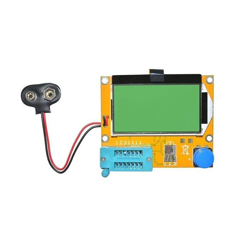
LCR-T4 Transistor Tester – Graphical LCD Meter
Measure hFE of your BC547 or 2N2222 transistors to find matched pairs for current mirror circuits. Also tests resistors, capacitors, and diodes — essential for the analog electronics workbench.
Building and Testing a Current Mirror
Here is a complete step-by-step guide to building a basic 1mA NPN current mirror on a breadboard:
Components Needed
- 2× BC547 NPN transistors (select from the same pack for best matching)
- 1× 10kΩ resistor (Rref, sets ~1.1mA reference)
- 1× 1kΩ–10kΩ resistor (as load RL for Q2 output)
- 12V power supply or 9V battery
- Multimeter (to measure current)
- Breadboard and jumper wires
Assembly Steps
- Insert both BC547 transistors into the breadboard, flat face towards you. Pin order: Collector (left), Base (centre), Emitter (right).
- Connect both Emitters to GND.
- Connect both Bases together (short with jumper wire).
- Connect Q1 Collector to Q1 Base (diode connection — the reference transistor).
- Connect Rref (10kΩ) from VCC to Q1 Collector/Base junction.
- Connect RL (load resistor, e.g. 4.7kΩ) from VCC to Q2 Collector.
- Connect multimeter in ammeter mode between Q2 Collector and RL to measure Iout.
Verification
With 12V supply and Rref = 10kΩ: Expected Iref ≈ (12–0.7)/10k = 1.13mA. Expected Iout ≈ 1.13mA (±5% for matched BC547 pair). Try different RL values (1kΩ, 4.7kΩ, 10kΩ) and verify Iout stays approximately constant — this confirms current source behavior. If Iout changes significantly with RL, verify Q2 is not saturating (check VCE(Q2) > 0.5V with multimeter).
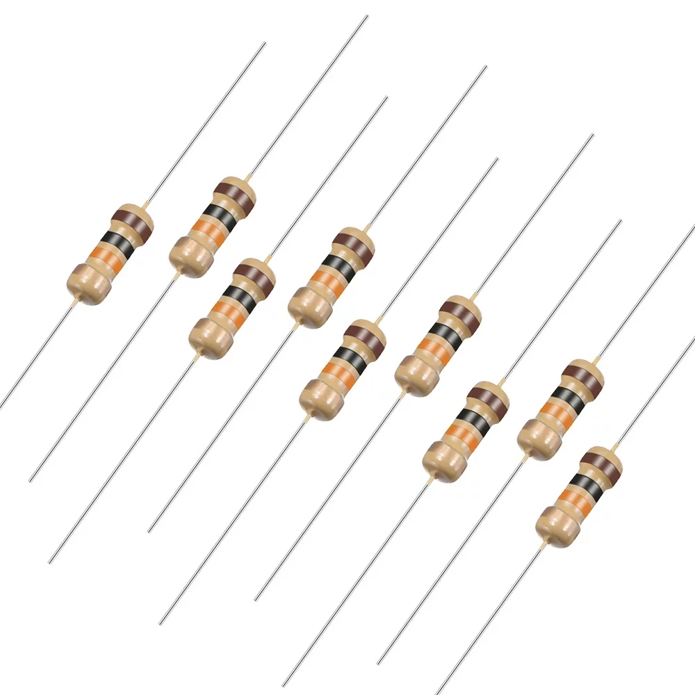
10 Ohm 0.25W Carbon Film Resistor (Pack of 50)
Small-value resistors for emitter degeneration in Widlar current mirrors, or as emitter resistors for current sensing in high-accuracy mirror circuits.
10CM Male To Male Breadboard Jumper Wires – 40Pcs
Essential for breadboarding current mirror and transistor biasing circuits. Good quality wires with firm connections for reliable analog circuit testing.
Frequently Asked Questions
Q1: Can I build a current mirror with a BC547 and BC557 (complementary pair)?
A PNP current mirror uses P-type transistors like BC557. The circuit is the mirror image of the NPN version — the reference transistor is diode-connected with its collector at VCC, and the emitters connect to VCC through Rref. PNP mirrors are used to create current sources that pull current from the positive supply rather than sinking to ground. Complementary mirrors (NPN + PNP) form the basis of class-AB output stages in power amplifiers.
Q2: How do I get Iout = 2× Iref (ratio current mirror)?
Use two Q2 transistors in parallel (both collectors tied together, both sharing the same base as Q1). Two identical transistors in parallel effectively create a transistor with 2× the emitter area, passing 2× the current for the same VBE. This gives Iout = 2 × Iref. For ratio N, use N output transistors in parallel or, for IC design, use a transistor with N× the emitter area.
Q3: Why don't we just use a resistor as a current source?
A resistor does provide a rough current, but it is not a true current source. With a resistor, Iout = (VCC – Vload) / R — if Vload changes (as the load impedance changes), Iout changes significantly. A current mirror maintains Iout nearly constant over a wide range of output voltages, which is essential for differential pair biasing, LED drivers, and DAC reference currents where load conditions vary.
Q4: What is output compliance voltage of a current mirror?
The output compliance voltage is the range of output voltage over which the current mirror maintains accurate current. For an NPN mirror with the output transistor in active region, compliance range is from VCE_sat (~0.2V) to (VCC – some margin). Outside this range, the transistor saturates (lower end) or breaks down (upper end), and current accuracy is lost.
Q5: Do real-world IC op-amps use current mirrors internally?
Yes, extensively. The LM741 uses a Widlar mirror for the differential pair tail current. The LM324 uses multiple current mirrors in its input stage, compensation stage, and bias network. Modern CMOS op-amps like the OPA2134 use cascoded MOSFET current mirrors for extremely high output impedance (and thus very high open-loop gain). Understanding current mirrors helps you read and understand op-amp datasheets and internal schematics, making you a far more effective analog electronics designer.
Explore Analog Electronics with Zbotic
Get transistors, resistors, capacitors, testing equipment, and all components needed for your analog circuit experiments — delivered fast anywhere in India from Zbotic.in.


Add comment