
Voltage Clamp Circuit: Diode Clipping and Clamping Guide
Every electronics circuit needs protection from unexpected voltage spikes — whether from switching transients, inductive kickback, ESD, or accidentally reversed power connections. A well-designed voltage clamp circuit using diodes is your first line of defence, quietly absorbing dangerous voltage excursions before they can destroy sensitive components. In this guide, we’ll cover every major type of clamping and clipping circuit, explain the theory clearly, and give you practical designs you can immediately build for your Arduino, Raspberry Pi, and microcontroller projects.
Clamping vs Clipping: Understanding the Difference
The terms “clipping” and “clamping” are often confused, but they describe two quite different operations on a waveform:
| Property | Clipping Circuit | Clamping Circuit |
|---|---|---|
| What it does | Removes (clips) peaks beyond a threshold | Shifts waveform DC level without changing shape |
| Waveform shape | Peaks are flattened/removed | Shape preserved, DC level shifts |
| Energy handling | Excess energy dissipated in diode/resistor | Capacitor stores and releases charge |
| Key component | Diode (forward or reverse biased) | Diode + Capacitor combination |
| Common uses | Overvoltage protection, waveform shaping | DC restoration, AC-to-DC offset, envelope detection |
Think of it this way: a clipper is like a pair of scissors that cuts off the tops of waves. A clamper is like a jack that lifts the entire wave up or pushes it down by a fixed amount, preserving every peak and valley of the original shape.
Diode Clipping Circuits: How They Work
A diode clipper uses the forward voltage drop characteristic of a diode (approximately 0.7 V for silicon) to limit signal voltage. When the input signal exceeds the threshold set by the diode orientation and any reference voltage, the diode conducts and clamps the output to the threshold level.
Single Positive Clipper
The simplest clipper: a series resistor (1 kΩ) followed by a diode connected from the signal node to GND (cathode to signal, anode to GND). When the signal goes positive and exceeds +0.7 V, the diode conducts and holds the output at approximately +0.7 V. Negative portions pass through unchanged.
Use case: Protecting an ADC input that expects signals in the 0–3.3 V range from accidental positive spikes above 3.3 V. Add a reference voltage (e.g., 3.3 V) in series with the diode to shift the clip level.
Dual (Bilateral) Clipper
Two diodes — one conducting for positive peaks, one for negative peaks — create a symmetric clipper. This is extremely common for protecting audio inputs, sensor inputs, and communication line interfaces.
Configuration: Signal → R1 (1 kΩ) → output node. D1: anode to output node, cathode to V+ (e.g., 5 V). D2: cathode to output node, anode to GND. This clips positive peaks above 5.7 V and negative peaks below -0.7 V.
Zener Clipper
For clipping at precise voltages above 0.7 V, use Zener diodes. A back-to-back Zener clipper (two Zeners in series, opposing polarity) clips at ±(Vz + 0.7) V. For example, two 5.1 V Zener diodes in series back-to-back will clip at ±5.8 V — useful for protecting RS-485/RS-232 transceiver inputs.
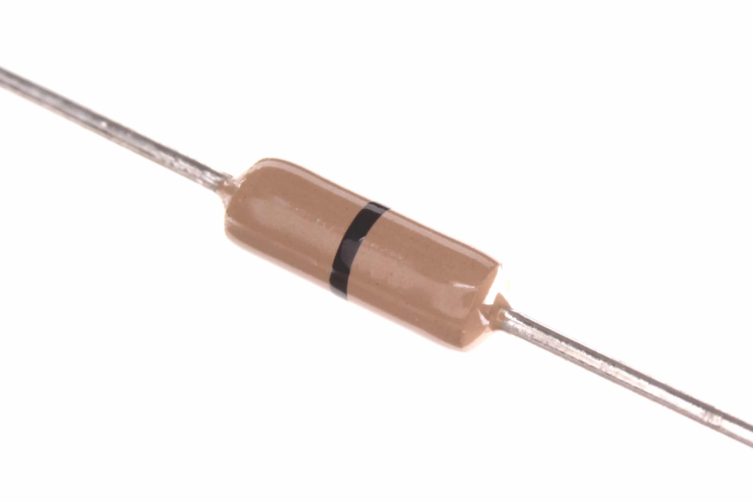
Carbon Film Resistors (Pack of 100)
Series resistors are critical in clipping circuits — they limit current through the diode when it conducts. Stock a variety of resistor values for your protection circuit designs.
Diode Clamping Circuits: DC Restorer Explained
A diode clamp (also called a DC restorer) shifts the DC level of an AC signal. It uses a diode and a capacitor working together: the capacitor charges to the peak of the input signal in one direction, and thereafter acts as a battery that offsets the entire waveform.
Positive Clamper (Shifts waveform UP)
Circuit: Input signal → C1 (coupling capacitor, e.g., 10 µF) → output. Diode D1: anode to GND, cathode to junction of C1 and output.
Operation: During the negative half-cycle of the input, D1 conducts and charges C1 to the peak negative voltage. During the positive half-cycle, D1 is reverse-biased and C1’s stored voltage adds to the input, pushing the output positive. Result: the entire waveform is shifted upward so the most negative point just touches 0 V (less D1 drop ≈ 0.7 V).
Example: A ±5 V sine wave fed through a positive clamper becomes approximately 0.7 V to 10.7 V at the output. The waveform shape is completely unchanged — only the DC level has shifted.
Negative Clamper (Shifts waveform DOWN)
Reverse the diode: anode to junction, cathode to GND. Now the capacitor charges during the positive half-cycle, and the output waveform is shifted so the most positive peak just touches 0 V.
Clamping to an Arbitrary Reference Voltage
Replace the GND reference with any DC voltage to clamp to that level instead. For example, clamping to 3.3 V ensures the output never goes below 3.3 V — useful for level-shifting a ±5 V signal into the 0–3.3 V range acceptable to an ESP32 ADC input.
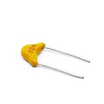
100nF Multilayer Ceramic Capacitor (Pack of 50)
Ceramic capacitors are ideal for high-frequency clamping circuits where low ESR matters. Use them in clamp circuits to handle fast voltage transients effectively.
Zener Diode Clamping for Precise Voltage Limiting
Zener diodes are designed specifically to operate in reverse breakdown at a precise, stable voltage — making them ideal for voltage clamping applications. Unlike a standard rectifier diode that only clamps at ~0.7 V forward voltage, a Zener clamps at its breakdown voltage (Vz), which is available from as low as 2.4 V to hundreds of volts.
Simple Zener Voltage Clamp
Place a Zener diode in parallel with the circuit you want to protect, with the cathode connected to the positive rail:
- Series resistor R1 from input source to Zener anode/cathode junction
- Zener diode: anode to GND, cathode to protected node
- Load connected between protected node and GND
When input voltage exceeds Vz, the Zener conducts in reverse breakdown and holds the output voltage at Vz. The series resistor R1 limits current through the Zener.
Sizing R1: R1 = (V_in_max − Vz) / I_z_max
For a 5.1 V Zener clamping a 12 V source: R1 = (12 − 5.1) / 0.02 = 345 Ω → use 330 Ω. Power dissipation in R1 = (12−5.1)² / 330 = 144 mW → use 1/2W resistor.
Bidirectional Zener Clamp
For AC signals or signals that can swing both positive and negative: connect two Zener diodes back-to-back (anode to anode, or cathode to cathode). This creates a symmetrical clamp at ±Vz levels. When signal exceeds +Vz, one Zener operates in breakdown while the other conducts forward. Vice versa for negative signals.
This is the circuit used inside virtually every chip input protection structure — replicated on-chip with junction diodes tied to VDD and VSS rails.
TVS Diodes: Fast Transient Protection
TVS (Transient Voltage Suppressor) diodes are optimised specifically for clamping fast voltage transients — ESD (electrostatic discharge), lightning surges, and inductive switching spikes. They respond in picoseconds, far faster than standard Zener diodes.
Key differences vs standard Zener:
- Much higher peak power: TVS diodes can absorb hundreds to thousands of watts for microsecond pulses
- Wider Vz tolerance: Typically ±5–10% vs ±2–5% for precision Zeners
- Not for DC regulation: Use Zeners for DC clamping; TVS for transient suppression
For protecting an ESP32 or Arduino GPIO pin from ESD: place a unidirectional 3.3 V TVS diode (e.g., SMAJ3.3A) between the input pin and GND. During normal operation it’s invisible. If a spike appears, it clamps within picoseconds. Series a 100 Ω resistor to limit current during clamping.
Overvoltage Protection Circuits for MCU Inputs
One of the most practical applications of voltage clamping in hobbyist projects is protecting 3.3 V microcontroller inputs from 5 V sensors, inadvertent wiring mistakes, or industrial signal levels.
Circuit 1: Dual-Diode Clamp to Supply Rails
The standard protection for every MCU GPIO pin:
- D1: anode to input signal line, cathode to VCC (3.3 V) — clamps positive overvoltage
- D2: anode to GND, cathode to input signal line — clamps negative undervoltage
- R1: 1 kΩ series resistor between external signal and the protected node
This allows the signal to swing freely between 0 V and 3.3 V. If it goes below -0.7 V or above 4 V (3.3 + 0.7), the appropriate diode conducts and clamps it. The 1 kΩ series resistor limits the clamping current to a safe level for both the diode and the MCU’s internal ESD structure.
Circuit 2: Level Shifting 5 V to 3.3 V with Resistor Divider + Clamp
For a 5 V digital signal driving a 3.3 V GPIO:
- Voltage divider: 10 kΩ from signal, 20 kΩ to GND → output ≈ 3.33 V for 5 V input
- Add a Schottky diode (BAT43 or similar) from divider output to 3.3 V rail for hard clamping
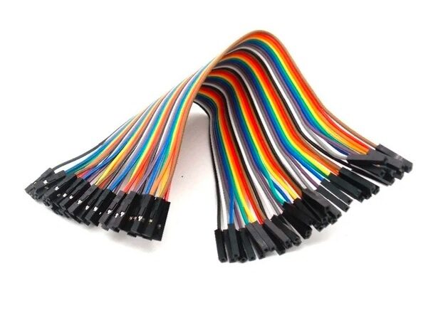
Female-to-Female Breadboard Jumper Wires 40Pcs
Prototype your voltage clamping and protection circuits quickly on a breadboard with these quality jumper wires. 10 cm length is perfect for compact circuit layouts.
Practical Design Examples
Design 1: Arduino Analog Input Protection for Industrial Sensors
Many industrial sensors output 0–10 V or 4–20 mA signals. To safely read a 0–10 V signal with an Arduino Uno (max 5 V ADC input):
- Voltage divider: 10 kΩ + 6.2 kΩ → 10 V becomes 3.8 V (within range)
- Series 1 kΩ resistor before ADC pin
- Zener diode (5.1 V) from ADC pin to GND — protects against wiring errors up to 50+ V
- 100 nF ceramic cap from ADC pin to GND — filters noise and protects against fast spikes
This four-component input stage can protect against mistakes that would otherwise destroy the MCU instantly.
Design 2: Relay Flyback Clamp
When a relay coil (12 V, 400 mH) is de-energised, it generates a spike of typically 50–100 V lasting 1–5 ms. A 1N4007 diode in reverse across the coil (cathode to +12 V, anode to transistor collector) clamps this spike to +12.7 V — completely protecting the switching transistor.
Design 3: Bidirectional Clamp for RS-232 Interface
RS-232 signals swing between -15 V and +15 V, but UART inputs on microcontrollers accept only 0–3.3 V. A MAX3232 IC handles this, but if you need a quick discrete solution:
- Series 10 kΩ resistor
- Two Zener diodes back-to-back (3.3 V) at the output
- Result: signal clipped to ±3.3 V maximum
- Note: This is a clipper, not a true level shifter — only works for digital data where peak level isn’t critical

0.1µF Ceramic Capacitor (Pack of 50)
Ceramic bypass capacitors are essential companions to diode clamping circuits — they filter high-frequency transients and provide a low-impedance path for noise to GND.
Frequently Asked Questions
Q1: Can I use an LED as a voltage clamp diode?
Yes, but it’s unusual. An LED has a forward voltage of 1.8–3.5 V depending on colour (red ≈ 1.8 V, blue/white ≈ 3.2 V), which can be used as a clamp reference. The LED will light up when clamping occurs, giving you a visual fault indicator. However, LEDs have limited current handling and are more expensive than 1N4148 diodes — use them only when the visual indication is useful.
Q2: What is the difference between a Schottky diode and a silicon diode for clamping?
Schottky diodes (like BAT43, 1N5819) have a forward voltage of only 0.2–0.4 V compared to 0.7 V for silicon diodes. They also switch much faster. Use Schottky diodes when you need clamping at lower voltages (to reduce Vforward drop in the protection level) or in high-frequency circuits where fast recovery is important. Silicon diodes (1N4148, 1N4007) are cheaper and handle higher voltages.
Q3: Why do I need a series resistor with a clamp diode?
Without a series resistor, when the clamp diode conducts, the input source drives current directly through the diode with only its forward resistance (a few ohms) limiting current. This can cause hundreds of milliamps to flow, potentially damaging the source, the diode, or both. A series resistor (typically 100 Ω to 10 kΩ) limits the clamping current to a safe level while introducing minimal loading on normal signals.
Q4: My clamping circuit distorts the signal I’m trying to protect. Why?
If the series resistor is too large, or if the diode’s junction capacitance is significant relative to the signal frequency, the RC network formed by the resistor and diode capacitance will roll off high-frequency components. Use a smaller series resistor (or a lower-capacitance Schottky diode) if signal integrity at high frequencies matters. Also ensure your clamping threshold is set correctly — if it’s too close to the normal signal peak, the diode will conduct slightly on every cycle.
Q5: Is a TVS diode better than a Zener diode for all protection applications?
Not necessarily. TVS diodes are optimised for fast, high-energy transients (ESD, lightning, inductive spikes). They are physically larger, more expensive, and have looser voltage tolerances. For slow, sustained overvoltage conditions, a Zener diode provides more precise clamping. For the best of both worlds, use a TVS diode at the circuit input (for ESD/spike protection) followed by a Zener diode for precision voltage clamping.
Protect Your Projects Before It’s Too Late
A burned microcontroller, a destroyed sensor, or a fried GPIO pin — all preventable with a ₹5 diode and a 1 kΩ resistor. Add voltage clamping to every external interface in your projects. Zbotic stocks all the diodes, capacitors, and resistors you need for comprehensive circuit protection.


Add comment