
Switching Power Supply Design: Flyback Topology Guide
The switching power supply flyback converter is arguably the most widely used isolated DC-DC topology in consumer electronics. From phone chargers to industrial control panels, from CCTV power adapters to Arduino shields — the flyback converter’s combination of simplicity, isolation, and multi-output capability makes it the go-to choice for millions of designs. In this comprehensive guide, we break down the flyback topology for Indian engineers and makers: from the fundamental energy transfer mechanism to transformer design, snubber circuits, and controller IC selection.
What Is a Flyback Converter?
A flyback converter is a type of isolated DC-DC switching power supply that stores energy in a transformer’s core during the switch-on phase and transfers it to the secondary (output) side when the switch turns off. The name “flyback” comes from the CRT television era — it refers to the brief, high-voltage pulse generated when the horizontal deflection circuit switches off (the “flyback” of the electron beam).
What makes the flyback uniquely valuable:
- Galvanic isolation: Input and output are electrically isolated — essential for mains-powered supplies, safety-critical applications, and noisy environments
- Multiple outputs: A single flyback transformer can have multiple secondary windings, each producing a different voltage — one transformer can generate +5V, +12V, and -12V simultaneously
- Wide input range: Handles wide input voltage variation (e.g., 85–265V AC after rectification) without topology change
- Low component count: Just one switch (MOSFET), one transformer, one diode, and output filter per output rail
- Low power sweet spot: Ideal for 1W to 150W output power — beyond that, forward or full-bridge topologies are more efficient
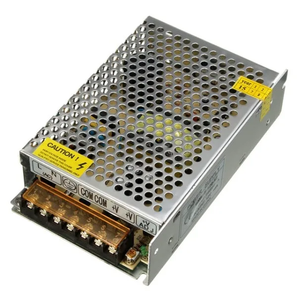
12V 10A SMPS – 120W DC Metal Power Supply
A ready-to-use switching power supply using flyback topology internally. Ideal for learning, testing, and powering your projects directly from the mains.
How the Flyback Converter Works
Unlike a conventional transformer that transfers energy simultaneously from primary to secondary, the flyback transformer stores energy in its core and releases it alternately. Technically, it acts more like a coupled inductor than a true transformer. This “energy bucket” mechanism is the heart of the flyback operation.
Phase 1: Energy Storage (Switch ON)
When the primary MOSFET switches on:
- Current flows from the DC bus through the primary winding, ramping up linearly
- Energy is stored in the transformer core’s magnetic field: E = 0.5 × L × I²
- The secondary diode is reverse-biased (the dots on primary and secondary are wound so that primary current flowing in creates reverse voltage on secondary)
- The output capacitor supplies load current during this phase
Phase 2: Energy Transfer (Switch OFF)
When the MOSFET turns off:
- The magnetic field in the core collapses — but inductor current cannot change instantaneously
- Voltage on the transformer reverses (“flies back”) — now the secondary diode becomes forward biased
- Energy stored in the core transfers to the secondary side, charging the output capacitor and supplying load current
- The primary MOSFET must withstand the reflected output voltage (Vout × Np/Ns) plus the DC bus voltage plus any leakage inductance spike
Voltage Transfer Ratio
In Discontinuous Conduction Mode (DCM):
Vout = Vin × D × √(Ton / (2 × L × f × Iout))
In Continuous Conduction Mode (CCM), the simpler approximation:
Vout / Vin = (Ns / Np) × D / (1 – D)
Where Np = primary turns, Ns = secondary turns, D = duty cycle.
Flyback Transformer Design: The Key to Everything
The transformer is the most critical component in a flyback converter. Getting the design wrong leads to core saturation, overheating, excessive EMI, or poor regulation. Here is a systematic design procedure:
Step 1: Define Operating Conditions
Example: 12V/5A (60W) output from 100–240V AC input (rectified to ~140–340V DC):
- Vin_min = 140V DC, Vin_max = 340V DC
- Vout = 12V, Iout = 5A, Pout = 60W
- Assumed efficiency η = 85%: Pin = 60 / 0.85 ≈ 70.6W
- Maximum duty cycle D_max = 0.45 (typically limited to 0.45–0.5 for stability margin)
- Switching frequency f = 65 kHz (common for EE/ETD ferrite cores)
Step 2: Calculate Primary Inductance
Peak primary current at minimum input and maximum duty cycle:
Ip_peak = 2 × Pin / (Vin_min × D_max) = 2 × 70.6 / (140 × 0.45) = 2.24A
Primary inductance for DCM operation (KRF = ripple factor ≈ 0.4):
Lp = Vin_min² × D_max² / (2 × Pin × f × (1 + KRF)) ≈ 300–500 µH
The exact value depends on your DCM/CCM operating choice — use simulation tools (LTspice, Webench) to verify.
Step 3: Select Core and Determine Turns
For 60W at 65 kHz, an EE35 or ETD39 ferrite core with N87 or N67 material is appropriate. Using the core’s Ae (effective area) and the winding formula:
Np = Vin_min × D_max / (Bpeak × Ae × f)
With Bpeak = 0.25T (well below saturation for N87 at 100°C), Ae ≈ 123 mm² for EE35:
Np = 140 × 0.45 / (0.25 × 123e-6 × 65000) ≈ 31.5 → use 32 turns
Turns ratio for 12V output (plus diode drop ≈ 0.7V, plus regulation margin ≈ 1.3V):
Ns = Np × (Vout + Vf) / (Vin_min × D_max / (1 – D_max)) = 32 × 13 / 114 ≈ 3.6 → use 4 turns
Step 4: Air Gap
The flyback transformer requires an air gap in the core to store energy (like an inductor). The gap length:
lgap = (µ0 × Np² × Ae) / Lp ≈ 0.3–0.8 mm
Air-gapped ferrite cores are available off-the-shelf from Epcos/TDK, Magnetics Inc., and local transformer suppliers in markets like Nehru Place (Delhi) or Lamington Road (Mumbai).
Step 5: Wire Gauge
Use current density of 3–5 A/mm² for the winding copper area. For 5A secondary:
Minimum wire area = 5 / 4 = 1.25 mm² → approximately 1.25 mm diameter enamelled copper wire for the secondary.

0.1MM Copper Enamelled Repair Reel Wire
Fine enamelled copper magnet wire for hand-winding flyback transformer primaries and auxiliary windings. Ideal for low-current auxiliary rails.
Snubber and Clamp Circuits
The leakage inductance of the flyback transformer stores energy that cannot be transferred to the secondary. When the MOSFET turns off, this energy produces a large voltage spike across the switch — potentially 2–3× higher than the DC bus voltage. Without protection, this destroys the MOSFET. Three protection methods are commonly used:
1. RCD Snubber (Most Common)
A resistor-capacitor-diode network across the primary MOSFET (drain to drain of the primary) clamps the voltage spike. The diode conducts during the spike, charging the capacitor, and the resistor dissipates the stored energy as heat.
- Simple and cheap
- Snubber dissipation = 0.5 × Lleak × Ip_peak² × f (can be significant at high power)
- Design trade-off: smaller Cs = better efficiency but higher spike voltage
2. TVS Diode (Transient Voltage Suppressor)
A TVS diode rated at Vin_max + 20% across the MOSFET clamps spikes hard. Fast response, but TVS must absorb all leakage energy as heat — suitable only for low-power designs under 10W.
3. Active Clamp Circuit
An additional MOSFET and capacitor recover the leakage inductance energy and feed it back to the input capacitor. This is the most efficient snubber approach — used in high-efficiency flyback designs (>90% efficiency) at the cost of an additional switch and gate driver.
4. Coupled Clamp (Zener Clamp)
A Zener diode in series with a diode across the primary winding clamps to a specific voltage. Simple, but Zener power dissipation must be managed.
Controller IC Selection
The controller IC drives the primary MOSFET at the correct duty cycle to regulate output voltage. The feedback path uses an optocoupler to cross the isolation barrier.
Popular Flyback Controller ICs in India
| IC | Type | Power Range | Key Feature |
|---|---|---|---|
| UC3842/UC3843 | Current mode | 5–100W | Classic, widely available, DIP-8 |
| NCP1200/NCP1380 | Current mode | 10–30W | Built-in MOSFET, ideal for chargers |
| TNY268/TNY278 | Off-line switcher | 4–23W | All-in-one: controller + MOSFET + protection |
| ICE3B1565 | Current mode | 50–150W | Soft-start, OCP, OVP built in |
| STR-A6069H | Quasi-resonant | 45–100W | High efficiency, QR valley switching |
For first-time flyback builders, the UC3842/UC3843 is recommended — it’s inexpensive, very well documented, available from dozens of Indian distributors, and has a massive community knowledge base. The more integrated TNY series is better if you want to minimise component count for a compact charger design.
CCM vs DCM Operation
The choice between Continuous Conduction Mode (CCM) and Discontinuous Conduction Mode (DCM) significantly affects transformer size, efficiency, and control complexity.
DCM (Discontinuous Conduction Mode)
In DCM, the inductor current reaches zero before the next switching cycle begins. The core completely demagnetises each cycle.
- Advantages: Simpler control loop (no RHP zero), lower primary current ripple at light loads, easier to achieve stability
- Disadvantages: Higher peak currents → larger core needed, more EMI, diode reverse recovery stress
- Best for: Low to medium power (under 50W), wide input voltage range, first-time designs
CCM (Continuous Conduction Mode)
In CCM, inductor current never reaches zero — it has a continuous DC component plus AC ripple.
- Advantages: Lower peak currents for same power, smaller core possible, lower EMI peak
- Disadvantages: RHP zero makes control loop compensation harder, diode reverse recovery is an issue, transformer must not saturate at start-up or transients
- Best for: Medium to high power (50W+), narrow input range, experienced designers
BCM/QR (Boundary/Quasi-Resonant Mode)
A third mode where the converter operates exactly at the boundary of DCM/CCM. Valley switching (triggering the MOSFET at the first voltage valley after resonant ringing) minimises switching losses. This is what high-efficiency laptop chargers (95%+ efficiency) typically use. QR controller ICs include the STR-A series from Sanken and the NCP1380 from onsemi.
PCB Layout Best Practices
Flyback converters involve high voltages and fast switching — PCB layout critically affects safety, efficiency, and EMI compliance. Here are the non-negotiable layout rules:
Creepage and Clearance
For mains-connected designs, maintain minimum 6mm creepage distance and 4mm clearance between primary and secondary traces. This is a safety requirement under IEC 60950/62368. Mark the isolation boundary clearly on your PCB silkscreen.
Primary Loop Minimisation
The primary switching loop (DC bus cap → transformer primary → MOSFET → current sense resistor → ground → back to cap) must be as short and compact as possible. This is the noisiest part of the circuit and the main EMI source.
Grounding
Use separate primary and secondary ground planes. Connect them only at the Y-capacitor tie point (for common-mode EMI filtering). Never let secondary ground traces run under the primary switching node area.
Optocoupler Placement
Place the feedback optocoupler physically at the isolation boundary, with its primary pin traces going to the primary side and secondary pins routed on the secondary side. Keep the optocoupler signal traces away from noisy switching nodes.
Snubber Component Placement
The RCD snubber components (R, C, D) must be placed as close as possible to the MOSFET drain and transformer primary pin. Any stray inductance in the snubber loop reduces its effectiveness and adds to the voltage spike.

10 x 10 cm Universal PCB Prototype Board Single-Sided
Prototype your flyback converter layout before ordering custom PCBs. Standard 2.54mm pitch for easy through-hole component placement.

6 Flexible Arms Soldering Station With Swiveling Alligator Clip
Hold your PCB, wires, and components steady while soldering your flyback converter prototype. Six flexible arms with alligator clips for hands-free assembly.
Frequently Asked Questions
Q1: Why is a flyback transformer not a real transformer?
A conventional transformer transfers energy from primary to secondary simultaneously. In a flyback converter, the primary stores energy in the core gap when the switch is ON, then releases it to the secondary when the switch is OFF. Primary and secondary never conduct at the same time. This is why the component is technically a “coupled inductor” rather than a true transformer — it uses the core for energy storage, not just magnetic coupling.
Q2: How do I calculate the voltage stress on the primary MOSFET?
The peak MOSFET drain voltage is: Vds_peak = Vin_max + Vreflected + Vspike. Vreflected = Vout × (Np/Ns). Vspike from leakage inductance is typically 20–50% of Vin_max. For a 265V AC input (375V DC), with 100V reflected and 100V spike, the MOSFET must withstand 575V. Use an 800V–1000V MOSFET for safe margin. Common choices: STF12N80, IRF840.
Q3: What causes a flyback converter to whistle or make noise?
Audible noise from a flyback converter is caused by magnetostrictive forces in the ferrite core vibrating at the switching frequency or sub-harmonic frequencies. If switching frequency is 20 kHz (at the edge of hearing) or lower, you’ll hear it. Solutions: increase switching frequency above 25 kHz, apply transformer varnish to damp mechanical resonance, use spread-spectrum frequency modulation to spread the acoustic energy, or better secure the transformer winding layers with tape before potting.
Q4: How do I add multiple output voltages to a flyback converter?
Add additional secondary windings to the transformer, each with its own diode and output capacitor. The turns ratio determines each output voltage. Only one output can be tightly regulated via feedback — the others will have “cross-regulation” error (they drift when load on the primary-regulated output changes). To improve cross-regulation: use coupled inductors or post-regulators (LDOs) on secondary outputs.
Q5: Is it safe to build a mains-connected flyback converter at home?
Working with mains voltage (230V in India) is potentially lethal. Always work with the converter powered off and capacitors discharged. Use an isolation transformer during testing. Never touch primary-side components with the mains connected. Consider starting with a low-voltage DC-input flyback (e.g., 12V input, regulated by an isolated DC-DC controller like the SG3525) before tackling mains-connected designs. Follow IS 616 (Indian Standard for safety of information technology equipment) for product design.
Build Your SMPS Project with Zbotic Components
Zbotic stocks capacitors, resistors, transistors, prototype boards, and soldering equipment to bring your switching power supply design to life. Whether you’re building a flyback charger, bench supply, or industrial SMPS, we have the parts you need with fast delivery across India.


Add comment