
Skin Effect in Conductors: High Frequency Design Impact
If you’re working with high frequency circuits, understanding skin effect in conductors is absolutely critical. At higher frequencies, alternating current doesn’t distribute evenly across the entire cross-section of a wire — instead, it crowds toward the outer surface. This skin effect in conductors at high frequency can dramatically increase effective resistance, cause unexpected signal losses, and ruin otherwise well-designed circuits. Whether you’re building RF amplifiers, switching power supplies, or high-speed digital PCBs in India, this guide will help you understand and mitigate skin effect for better designs.
What Is Skin Effect?
The skin effect is a phenomenon in which alternating current (AC) tends to flow near the outer surface of a conductor rather than through its entire cross-sectional area. At DC (zero frequency), current distributes uniformly across the full conductor cross-section, giving the lowest possible resistance. But as frequency increases, electromagnetic induction creates opposing currents in the conductor’s interior, effectively pushing the current toward the surface.
The physical explanation lies in Faraday’s law. The changing magnetic field inside the conductor induces eddy currents that oppose the primary current flow. The result is that current density is highest at the surface and decays exponentially as you move toward the center. By the time you’re a few “skin depths” below the surface, the current is negligible.
This matters enormously in practice. A copper wire that measures 10 mΩ at DC might present 100 mΩ or more at 1 MHz — a 10x increase in resistance — simply because only a thin annular shell of the conductor is actually carrying current. Power is dissipated in a smaller effective cross-section, leading to I²R losses and heat generation that circuit designers often don’t anticipate.
Skin Depth Formula and Calculation
The key parameter for quantifying skin effect is the skin depth (δ), which represents the depth at which the current density falls to 1/e (about 37%) of its surface value. The formula is:
δ = √(2ρ / ωμ) = √(ρ / (π × f × μ))
Where:
- δ = skin depth in metres
- ρ = resistivity of the conductor (Ω·m) — for copper: 1.72 × 10⁻⁸ Ω·m
- f = frequency in Hz
- μ = permeability of the conductor (H/m) — for copper: 4π × 10⁻⁷ H/m
Let’s calculate skin depth in copper at common frequencies:
| Frequency | Skin Depth (Copper) | Typical Application |
|---|---|---|
| 50 Hz (mains) | 9.3 mm | Power wiring — negligible skin effect |
| 1 kHz | 2.1 mm | Audio circuits |
| 100 kHz | 0.21 mm (210 µm) | Switching power supplies |
| 1 MHz | 66 µm | RF circuits, fast MCUs |
| 100 MHz | 6.6 µm | WiFi, Bluetooth, RF modules |
| 2.4 GHz | 1.35 µm | WiFi, ESP8266/ESP32 |
At 2.4 GHz — the frequency used by your ESP8266 or ESP32 module — the skin depth in copper is just 1.35 micrometres. A standard PCB trace is typically 35 µm thick (1 oz copper). This means current is flowing in only the top 4% of the trace’s thickness. The practical consequence: a wide trace doesn’t help much at microwave frequencies. What matters is the surface area and surface quality of the conductor.
How Frequency Affects Conductor Resistance
The AC resistance of a round conductor increases as frequency rises. In the low-frequency regime (where the wire diameter is much smaller than skin depth), resistance equals the DC resistance. As frequency increases and skin depth shrinks below the wire radius, resistance scales approximately as the square root of frequency:
R_AC ≈ R_DC × (a / 2δ) for a >> δ
Where a is the wire radius. In plain language: doubling the frequency increases AC resistance by about 41% (√2). Going from 1 MHz to 100 MHz increases AC resistance by a factor of 10.
For a concrete example relevant to Indian hobbyists: if you use standard 22 AWG copper wire (0.644 mm diameter) to carry a 1 MHz signal, the AC resistance is roughly 5× higher than at DC. At 10 MHz, it’s about 15× higher. This is why RF coil designers use Litz wire (multiple fine, individually insulated strands) — more surface area for the same total copper mass.
The proximity effect compounds skin effect in transformers and multi-wire situations. When two current-carrying conductors are placed near each other, their magnetic fields interact and further concentrate current to specific regions of each conductor, sometimes increasing effective resistance far beyond the isolated skin-effect calculation.
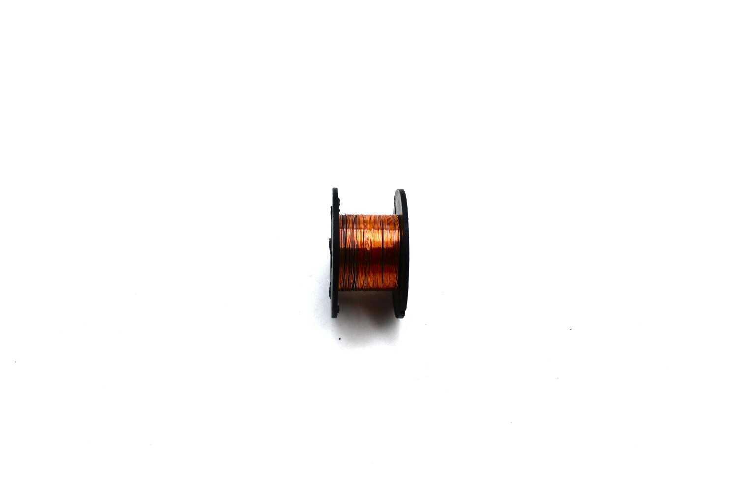
0.1MM Copper Enamelled Repair Reel Wire
Fine 0.1mm enamelled copper wire — ideal for winding RF coils and inductors where skin effect management matters. The thin gauge maximises surface-to-volume ratio and reduces AC resistance at higher frequencies.
Skin Effect in PCB Design
For PCB designers, skin effect is most relevant in the following scenarios:
High-Speed Digital Signals
Modern microcontrollers and FPGAs operate at clock frequencies of tens to hundreds of MHz. Even if your clock is 50 MHz, harmonics of digital signals extend well beyond the fundamental. A square wave at 50 MHz has significant energy at 150 MHz, 250 MHz, and beyond. PCB trace resistance at these harmonics is considerably higher than at DC, causing signal attenuation and edge degradation. For a 50-MHz clock trace longer than 5 cm, skin effect resistance becomes non-negligible.
RF Transmission Lines
Microstrip and stripline transmission lines on PCBs operate at frequencies where skin depth is a fraction of the copper thickness. Surface roughness becomes critical — a rough copper surface increases effective resistance because the actual current path is longer than a smooth surface would give. High-quality PCB copper (reverse-treated or VLP foil) has lower surface roughness and lower loss at GHz frequencies.
Power Inductors and Transformers
In switching power supplies (common in Indian DIY power projects), inductors switch at 100 kHz to 1 MHz. Skin effect in the winding wire causes core and copper losses that degrade efficiency. At 500 kHz, skin depth in copper is about 94 µm. Standard 0.5 mm (500 µm) diameter wire would see significant skin effect — only the outer 18% of diameter effectively carries current.
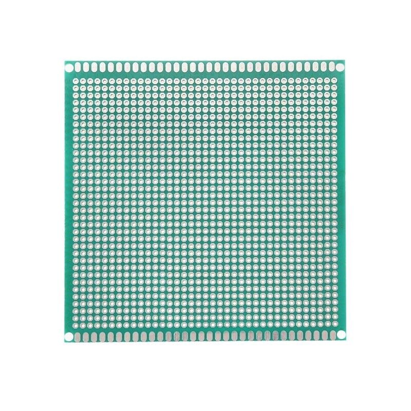
10 x 10 cm Universal PCB Prototype Board
Single-sided 2.54mm pitch prototype board for building and testing high-frequency circuit layouts. A great starting point before committing to a custom PCB fabrication.
Mitigation Strategies for High Frequency Designs
Now that you understand skin effect, let’s look at practical ways to work around it:
1. Use Litz Wire for RF Inductors
Litz wire consists of many thin, individually insulated strands twisted together. Because each strand is thinner than one skin depth, current distributes evenly among all strands. A bundle of 100 strands of 50 µm wire has much lower AC resistance at 1 MHz than a single 500 µm wire with the same total copper cross-section. For Indian hobbyists winding RF coils or high-frequency transformers, sourcing Litz wire can dramatically improve efficiency.
2. Wider Traces Are Better — Up to a Point
For PCB traces at moderate frequencies (1–10 MHz), wider traces reduce AC resistance. However, the benefit saturates because current flows only in the surface. For GHz frequencies, surface quality matters more than width.
3. Silver-Plate High-Frequency Connectors
Silver has slightly lower resistivity than copper (1.59 vs 1.72 × 10⁻⁸ Ω·m) and thus slightly greater skin depth. More importantly, silver-plated connectors present a high-conductivity surface where all the current flows. This is why RF connectors (SMA, BNC) use silver or gold plating.
4. Keep High-Frequency Traces Short
The simplest mitigation: reduce trace length. Every centimetre saved is a centimetre of elevated AC resistance eliminated. Keep RF components close together, and use ground planes aggressively to control impedance.
5. Use Ground Planes Correctly
A solid ground plane underneath your high-frequency traces returns current in a thin skin-effect layer on the ground plane’s surface. Breaks, slots, or vias in the ground plane force the return current to take longer paths, dramatically increasing loop inductance and skin-effect losses.
6. Choose the Right PCB Stack-up
For RF work above 500 MHz, consider specialised substrates like Rogers 4003C instead of standard FR4. FR4’s dielectric loss tangent (0.02–0.025) is significantly higher than Rogers (0.0027), though for frequencies below 1 GHz on a budget, FR4 is often acceptable.
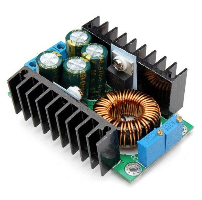
300W 10A DC-DC Step-down Buck Converter Module
A high-power adjustable buck converter — a great platform to study skin effect in switching circuits. The internal inductor and PCB traces handle high-frequency switching currents where skin effect losses are real.
Practical Examples for Indian Makers
Example 1: ESP32 WiFi Antenna Trace
Your ESP32 module operates at 2.4 GHz. At this frequency, skin depth in copper is about 1.35 µm. Standard PCB copper (35 µm, 1 oz) has more than enough thickness — the extra copper above 1.35 µm is essentially wasted for RF current. However, it still helps mechanically and for DC/low-frequency currents. The critical concern is the antenna trace impedance (typically 50 Ω microstrip) and keeping the ground plane continuous beneath it.
Example 2: Flyback Power Supply Transformer
A typical offline flyback converter (used in many Indian DIY lab PSU projects) switches at 60–100 kHz. Skin depth at 100 kHz is 210 µm. If you wind your transformer with 0.5 mm diameter wire, you’re past one skin depth — a significant fraction of the copper cross-section is underutilised. Using multiple parallel thinner wires (like three 0.2 mm wires instead of one 0.5 mm wire) will reduce winding resistance and improve efficiency.
Example 3: Audio Crossover Inductors
Audio crossover frequencies (1–10 kHz) give skin depths of 2.1–0.66 mm. For typical 0.5–1 mm diameter wire used in crossover inductors, skin effect is just beginning to matter at 5 kHz and above. For audiophiles building crossover networks, air-core inductors wound with flat (ribbon) copper conductors present more surface area per unit volume than round wire.
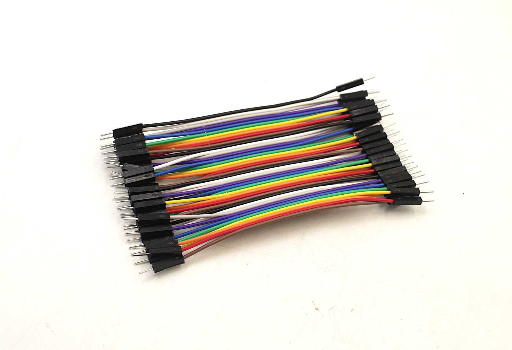
10CM Male To Male Breadboard Jumper Wires 2.54MM – 40Pcs
Flexible breadboard jumper wires for prototyping circuits. Keep them short when working with RF or high-speed signals — skin effect resistance adds up over longer wire runs.
Recommended Tools and Components
To experiment with skin effect and high-frequency design in your lab, here are some useful resources available in India:
- Online calculators: Chemandy Electronics skin effect calculator, Coil32 for inductor design with skin effect correction
- Simulation: LTspice (free) can model skin effect using lossy transmission line elements
- Measurement: An LCR meter or impedance analyser shows how inductance and resistance change with frequency — revealing skin effect directly
- PCB prototyping: Order 4-layer PCBs from JLCPCB or PCBWay (both serve India well) to experiment with ground planes and microstrip design
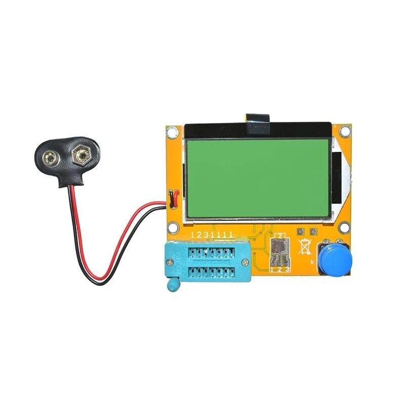
LCR-T4 12864 LCD Graphical Component Tester
Measure resistance, capacitance, inductance and ESR. A handy tool for characterising components and verifying inductor performance — useful when studying skin effect in hand-wound coils.
Frequently Asked Questions
Q: At what frequency does skin effect become important for a typical Arduino project?
For standard Arduino (16 MHz clock), the fundamental is 16 MHz with harmonics extending to 48 MHz and beyond. At 16 MHz, skin depth in copper is about 17 µm — significant relative to PCB trace thickness. For short traces (<2 cm) and moderate currents, it’s rarely a practical problem. But for clock distribution networks and fast edges, keep traces short and use a ground plane.
Q: Does skin effect affect DC power supply wiring?
At 50 Hz (Indian mains), skin depth in copper is 9.3 mm — larger than any practical wire diameter. Skin effect is completely negligible for mains power wiring. It only becomes significant above a few kilohertz.
Q: Can I reduce skin effect loss by using aluminium instead of copper?
Aluminium has higher resistivity (2.82 × 10⁻⁸ vs 1.72 × 10⁻⁸ Ω·m), so its skin depth is actually larger than copper at any given frequency. However, its absolute resistance per unit length is also higher. Overall, copper is the better choice for high-frequency applications. Silver is marginally better than copper but impractical for most applications due to cost.
Q: How does skin effect relate to the Q factor of an RF coil?
Q factor (quality factor) is directly affected by skin effect. As AC resistance increases with frequency due to skin effect, the Q factor decreases. High-Q inductors for RF use small-diameter Litz wire or air-core designs with silver-plated conductors to minimise AC winding resistance and maintain high Q.
Q: Is skin effect a concern for USB cables and HDMI cables?
Yes, to a degree. USB 3.0 and HDMI 2.0 operate at several Gbps, meaning signal frequencies in the GHz range. Cable designers account for skin effect and dielectric losses by specifying conductor material, plating, and insulation carefully. This is why high-speed cables are tested for insertion loss across a frequency range, not just at DC.
Build Better High-Frequency Circuits
Ready to put skin effect theory into practice? Zbotic stocks quality electronic components including copper wire, PCB prototyping boards, and test equipment for Indian makers and engineers. Explore our full range of electronics components and elevate your next RF or switching power design.


Add comment