
The common emitter (CE) amplifier is the workhorse of analogue electronics. It is one of the three fundamental BJT transistor configurations — and by far the most widely used for voltage amplification. From audio pre-amplifiers and radio receivers to sensor signal conditioning and logic-level shifting, the common emitter amplifier appears everywhere.
In this tutorial you will learn exactly how a CE amplifier works, how to calculate its voltage gain, input impedance, and output impedance, and how to design one from scratch using a simple and systematic approach. By the end, you will be confident enough to build and test your own amplifier on a breadboard.
What Is a Common Emitter Amplifier?
In a BJT (Bipolar Junction Transistor) amplifier, one of the three terminals — Base, Collector, or Emitter — serves as the common reference between the input and output. When the Emitter is the common terminal:
- Input signal is applied between Base and Emitter
- Output signal is taken between Collector and Emitter
- Emitter is common (AC ground) to both
Key characteristics of the common emitter configuration:
- Voltage gain: High (typically −50 to −300, sign indicates phase inversion)
- Current gain: High (≈ β or h_fe of the transistor)
- Phase: 180° inversion between input and output
- Input impedance: Moderate (a few kilohms)
- Output impedance: High (tens of kilohms)
Circuit Topology and Component Roles
A practical CE amplifier with voltage divider bias contains these components:
- V_CC: DC supply voltage (typically 5 V–15 V)
- R₁, R₂ (voltage divider): Set the base DC bias voltage. Choosing R₁ and R₂ correctly is the foundation of a stable design.
- R_C (collector resistor): Converts collector current variations into output voltage variations. Larger R_C = higher gain.
- R_E (emitter resistor): Provides DC stability against temperature and β variations. Bypassed by C_E for AC signals.
- C_E (emitter bypass capacitor): Short-circuits R_E at AC frequencies, preventing the AC gain from being reduced by negative feedback.
- C₁ (input coupling capacitor): Blocks DC from the signal source while passing the AC signal to the base.
- C₂ (output coupling capacitor): Blocks DC from appearing at the output while passing the amplified AC signal to the load.
DC Bias Analysis
For DC analysis, all capacitors are treated as open circuits. The goal is to set the transistor operating point (Q-point) in the active region, typically at V_CE ≈ V_CC/2 for maximum signal swing.
Voltage Divider Base Voltage
V_B = V_CC × R₂ / (R₁ + R₂)
Emitter Voltage and Current
V_E = V_B − V_BE  (V_BE ≈ 0.7 V for silicon NPN)
I_E = V_E / R_E
I_C ≈ I_E  (since β >> 1, I_C ≈ α × I_E ≈ I_E)
Collector-Emitter Voltage
V_C = V_CC − I_C × R_C
V_CE = V_C − V_E = V_CC − I_C(R_C + R_E)
For the Q-point to sit mid-way on the load line: V_CE ≈ V_CC/2.
Stability Condition
The voltage divider is considered “stiff” (insensitive to β variation) when:
R₁ ‖ R₂ ≤ β × R_E / 10
This ensures the divider current is at least 10× the base current, making V_B stable regardless of transistor β.
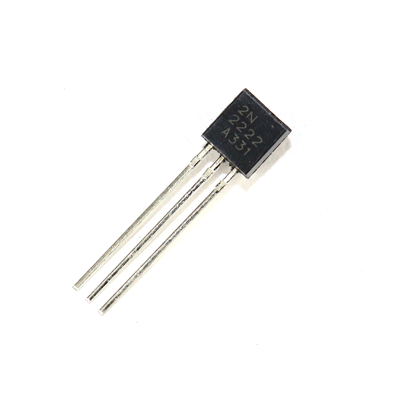
2N2222 NPN Transistor (Pack of 20)
The 2N2222 is a classic general-purpose NPN transistor — perfect for building common emitter amplifier prototypes with β (hFE) of 100–300 at typical bias currents.
AC Small-Signal Analysis
For AC analysis, replace:
- All capacitors → short circuits (assuming frequencies well above cut-off)
- DC voltage sources → short circuits (ideal voltage source = 0 Ω for AC)
- Transistor → small-signal T-model or hybrid-π model
The key small-signal parameter is the transistor’s transconductance g_m and emitter resistance r_e:
g_m = I_C / V_T  (V_T = 26 mV at room temperature)
r_e = V_T / I_C = 1/g_m
r_π = β / g_m = β × r_e
Voltage Gain Calculation
With Emitter Bypass (C_E in place)
When C_E bypasses R_E completely:
A_v = −g_m × (R_C ‖ R_L) = −(R_C ‖ R_L) / r_e
The minus sign indicates 180° phase inversion.
Example: I_C = 1 mA, R_C = 5 kΩ, R_L = 10 kΩ
r_e = 26/1 = 26 Ω
R_C ‖ R_L = (5k × 10k)/(5k + 10k) = 3.33 kΩ
A_v = −3330/26 = −128
Without Emitter Bypass (C_E removed)
Without C_E, R_E appears in the AC path and reduces gain but improves linearity and bandwidth:
A_v = −(R_C ‖ R_L) / (r_e + R_E)
With R_E = 1 kΩ added to the same example:
A_v = −3330 / (26 + 1000) ≈ −3.24
Gain drops dramatically but the circuit is much more stable and linear — used in precision applications.
Input and Output Impedance
Input Impedance (Z_in)
Z_in = R₁ ‖ R₂ ‖ (β × r_e)   [with C_E bypassing R_E]
Z_in = R₁ ‖ R₂ ‖ β(r_e + R_E) [without C_E]
For signal sources with high source impedance, a high Z_in is desirable (less signal loading).
Output Impedance (Z_out)
Z_out ≈ R_C (assuming r_o >> R_C, where r_o is transistor output resistance)
Typical Z_out is 1 kΩ–10 kΩ. If you need to drive a low-impedance load, follow the CE stage with a common-collector (emitter follower) stage to transform impedance.
Complete Design Example
Specifications:
- V_CC = 12 V
- Transistor: BC547 (β_min = 110)
- Desired I_C = 2 mA (Q-point)
- Desired voltage gain A_v ≥ −100
- Load R_L = 10 kΩ
- Signal frequency: audio (20 Hz – 20 kHz)
Step 1 — Choose R_C
For V_CE ≈ V_CC/2 = 6 V, allow 2 V across R_E:
V_RC = 12 − 6 − 2 = 4 V
R_C = V_RC / I_C = 4 / 0.002 = 2 kΩ → use 2.2 kΩ (standard)
Step 2 — Verify Gain
r_e = 26mV / 2mA = 13 Ω
R_C ‖ R_L = 2200 ‖ 10000 = 1803 Ω
A_v = −1803 / 13 ≈ −139  ✓ (exceeds −100 requirement)
Step 3 — Choose R_E
V_E = 2 V (chosen)
R_E = 2 / 0.002 = 1 kΩ
Step 4 — Choose R₁, R₂
V_B = V_E + 0.7 = 2 + 0.7 = 2.7 V
Choose divider current = 10 × I_B = 10 × (2mA/110) ≈ 182 µA
R₁ + R₂ = V_CC / I_divider = 12 / 182µ = 66 kΩ
R₂ = V_B / I_divider = 2.7 / 182µ = 14.8 kΩ → use 15 kΩ
R₁ = 66k − 15k = 51 kΩ → use 47 kΩ + 3.9 kΩ in series, or 56 kΩ
Step 5 — Choose Capacitors
Lower cut-off frequency f_L = 20 Hz
C₁: X_C1 ≤ Z_in/10 at 20 Hz
Z_in = 47k ‖ 15k ‖ (110 × 13) = 47k ‖ 15k ‖ 1430 ≈ 1280 Ω
C₁ ≥ 1/(2π × 20 × 128) ≈ 62 µF → use 100 µF

C_E: X_CE ≤ R_E/10 at 20 Hz
C_E ≥ 10/(2π × 20 × 1000) ≈ 80 µF → use 100 µF
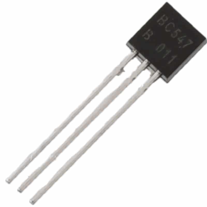
BC547 NPN 100mA Transistor TO-92 (Pack of 10)
The BC547 is ideal for the CE amplifier design example in this article — low noise, β of 110–800, and widely available in TO-92 package for easy breadboard insertion.
Frequency Response and Bandwidth
The CE amplifier does not amplify all frequencies equally. It has a band-pass characteristic:
- Low-frequency cut-off (f_L): Caused by coupling capacitors (C₁, C₂) and bypass capacitor (C_E). Below f_L, gain drops by 3 dB per pole.
- Mid-band: Flat gain region between f_L and f_H — the useful operating range.
- High-frequency cut-off (f_H): Caused by transistor junction capacitances (C_π, C_µ) and Miller effect. The Miller effect multiplies C_µ by (1 + |A_v|), making it the dominant high-frequency limitation.
Gain-Bandwidth Product (GBW) = |A_v| × f_H ≈ f_T (transit frequency of transistor)
For BC547: f_T ≈ 300 MHz
If |A_v| = 100 → f_H ≈ 300 MHz / 100 = 3 MHz
Practical Building Tips
- Use a breadboard first: Always prototype on a breadboard before soldering. Measure V_B, V_E, V_C with a multimeter to confirm the Q-point before applying any AC signal.
- Measure β first: Use an LCR/component tester to measure the actual β of your transistor before designing — β can vary 2:1 within the same part number.
- Watch for saturation: If V_CE drops below about 0.2 V, the transistor is saturated and the output will be clipped. Reduce the input signal amplitude or adjust R_C.
- Decouple the supply: Place a 100 nF ceramic capacitor close to V_CC pin on the breadboard to suppress high-frequency noise on the supply rail.
- Check DC first, AC second: Set up and verify the DC bias point completely before connecting any AC signal source.
- Input coupling: A 1 kΩ resistor in series with the signal source input protects the transistor from signal source shorts and prevents oscillation.
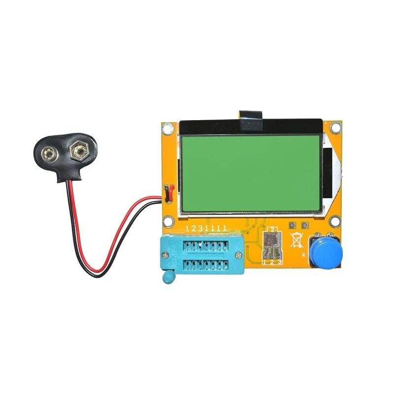
LCR-T4 12864 LCD Graphical Transistor Tester
Measure actual β (hFE), V_BE, and identify unknown transistors instantly — essential for accurate CE amplifier design and verifying component parameters before building.
Frequently Asked Questions
Why does the common emitter amplifier invert the output signal?
When the input voltage at the base increases, the base current increases, causing more collector current to flow. More collector current means a larger voltage drop across R_C, which reduces the collector voltage (V_C = V_CC − I_C × R_C). So when the input goes up, the output goes down — a 180° phase inversion.
What is the purpose of the emitter bypass capacitor?
The emitter bypass capacitor (C_E) short-circuits R_E at AC signal frequencies. This prevents the AC voltage gain from being reduced by the negative feedback that R_E would otherwise introduce. Without C_E, the gain is approximately −R_C/R_E; with C_E, it is approximately −R_C/r_e, which is much higher.
How do I choose the Q-point for a CE amplifier?
For maximum undistorted output swing, set V_CE ≈ V_CC/2. This centres the operating point on the AC load line. If you need to amplify small signals with low distortion but do not need maximum swing, you can choose a lower Q-point I_C to reduce power consumption.
What is the difference between common emitter, common base, and common collector?
Common emitter (CE) has high voltage gain and 180° phase inversion. Common base (CB) has high voltage gain with no phase inversion and very low input impedance. Common collector (CC, also called emitter follower) has voltage gain close to 1, no phase inversion, very high input impedance, and very low output impedance — used as a buffer stage.
Can a common emitter amplifier be used for audio?
Yes. CE amplifiers are widely used as pre-amplifier stages in audio circuits (microphone pre-amps, phono stages). For audio, careful attention to coupling capacitor values (to pass 20 Hz) and noise performance (choose low-noise transistors like BC547B or 2N3904) is important.
Why does gain decrease at high frequencies?
At high frequencies, the transistor’s internal junction capacitances (C_π and C_µ) begin to bypass the signal. The Miller effect multiplies C_µ by (1 + |A_v|), making it the dominant high-frequency limitation. This causes the gain to roll off at −20 dB/decade above the upper cut-off frequency f_H.
Build Your Own CE Amplifier Today
All the components you need — BC547 transistors, resistors, capacitors, jumper wires, and a power supply — are available at Zbotic. Follow the design example above, build it on a breadboard, and measure your gain with a multimeter or oscilloscope.


Add comment