
The Bipolar Junction Transistor is one of the most fundamental building blocks in electronics. Invented at Bell Labs in 1947, it enabled the miniaturisation of electronics that led to everything from pocket radios to modern CPUs. Yet despite its age, the BJT remains absolutely essential knowledge — it is still used in audio amplifiers, switching regulators, high-speed logic, and countless analog circuits where MOSFETs fall short.
The key to understanding any BJT circuit is knowing which region of operation the transistor is in at any given moment. A BJT in the wrong region can mean a logic gate that doesn’t switch cleanly, an amplifier that clips, or a transistor that dissipates dangerous amounts of power. This guide covers all three regions in depth, with practical circuit examples and the math you need to design real circuits.
1. BJT Structure and Types
A BJT consists of three semiconductor layers forming two p-n junctions:
- Emitter (E): Heavily doped, injects carriers into the base
- Base (B): Very thin (a few microns) and lightly doped; controls transistor action
- Collector (C): Moderately doped, collects carriers from the base
There are two polarities:
- NPN: N-type emitter, P-type base, N-type collector. Current flows into the base to allow collector-to-emitter current flow. Most common type.
- PNP: P-type emitter, N-type base, P-type collector. Current flows out of the base. Used as high-side switches and in complementary push-pull output stages.
The transistor’s key parameter is hFE (β — beta), the DC current gain: the ratio of collector current (I_C) to base current (I_B). Typical values range from 50 to 500, with datasheet values given at specific operating points. For circuit design, use β = 100 as a conservative estimate unless you have specific data.
2. The Three Regions of Operation
The BJT’s behaviour is determined by the bias state of its two p-n junctions — the Base-Emitter junction (VBE) and the Base-Collector junction (VBC):
| Region | B-E Junction | B-C Junction | Behaviour |
|---|---|---|---|
| Cutoff | Reverse biased | Reverse biased | OFF — no current flows |
| Active | Forward biased | Reverse biased | Amplifying — I_C = β × I_B |
| Saturation | Forward biased | Forward biased | ON — V_CE minimal (~0.2V) |
There is also a fourth region — Reverse Active — where the junctions are biased opposite to the Active region (B-E reverse, B-C forward). This is rarely intentional and results in very low gain. We will not cover it further.
3. Cutoff Region: The Open Switch
In the cutoff region, neither junction is forward biased. For an NPN transistor:
- VBE < 0.5V (junction not forward biased)
- I_B ≈ 0 (no base current)
- I_C ≈ 0 (only leakage current, typically nanoamperes)
- VCE ≈ VCC (the full supply voltage appears across the collector-emitter)
The transistor behaves like an open switch. No current flows from collector to emitter. The small leakage current (I_CEO) is negligible in most circuits.
This is the OFF state for digital switching applications. When the Arduino writes LOW to a base resistor circuit, VBE drops below ~0.5V and the transistor cuts off, de-energising the load.
Entering Cutoff
For reliable cutoff, ensure VBE < 0.3V. In circuits where the base might float (input disconnected), add a pull-down resistor (10kΩ–100kΩ) from base to emitter to guarantee VBE = 0V when no drive signal is present.

BC547 NPN 100mA Transistor TO-92 (Pack of 10)
The BC547 is the go-to NPN transistor for learning all three BJT regions of operation. Ideal for signal-level switching up to 100mA.
4. Active (Linear) Region: Amplification
The active region is where the transistor acts as a controllable current source. The base-emitter junction is forward biased (VBE ≈ 0.6–0.7V for silicon), and the base-collector junction is reverse biased (VBC < 0V for NPN).
In this region:
- I_C = β × I_B (collector current is β times the base current)
- I_E = I_C + I_B (KCL at the emitter node)
- VBE ≈ 0.6V–0.7V (fixed by the forward-biased junction)
- VCE must be > VCE_sat (typically >0.3V) to stay in active region
The remarkable property here is that a tiny base current (microamperes) controls a much larger collector current (milliamperes). This is transistor action — current amplification.
Early Effect (VA)
In practice, I_C increases slightly as VCE increases even at constant I_B. This is the Early Effect, characterised by the Early voltage V_A (typically 50–200V for BJTs). It creates a finite output resistance that matters in precision amplifier design but can be ignored in most switching applications.
Active Region Operating Point (Q-Point)
For amplifier design, you establish a DC Q-point (quiescent point) in the middle of the active region to allow the signal to swing both positive and negative without hitting cutoff or saturation. Typical target: VCE = VCC/2, I_C = a few milliamperes.
5. Saturation Region: The Closed Switch
In the saturation region, both junctions are forward biased. You have driven enough base current that the transistor is fully ON. Key characteristics:
- VCE_sat ≈ 0.1V–0.3V (very low — a near-closed switch)
- VBE_sat ≈ 0.7V–1.0V (slightly higher than in active region)
- I_C is determined by the external circuit (load resistance), NOT by β × I_B
- β is effectively reduced — the transistor is ‘over-driven’
The condition for saturation in a switching circuit:
I_B ≥ I_C / β_forced
Where β_forced is the forced beta — typically 10–20 (much less than the datasheet β). Using β_forced = 10 for design provides a safety factor ensuring reliable saturation even with part-to-part β variation.
Saturation Delay (Storage Time)
One consequence of deep saturation is that minority carriers are stored in the base region. When you turn the transistor OFF, these carriers must be removed before the transistor leaves saturation — this creates a storage time delay (typically 100ns–several µs). In high-speed switching circuits, avoid deep saturation by using Schottky clamps or current-limiting the base drive.
6. I-V Characteristic Curves Explained
The BJT’s output characteristics (I_C vs VCE at constant I_B) are the most useful graphical tool for understanding regions of operation:
- Bottom (I_C ≈ 0): Cutoff region — base current zero or below threshold
- Left side (VCE < ~0.3V): Saturation region — curves bunch together, I_C determined by external circuit
- Flat plateau region: Active region — family of nearly horizontal lines, each corresponding to a different I_B; spacing between lines = β
The load line is drawn on this graph representing the constraint imposed by the external circuit (Vcc, R_C). The intersection of the load line and an I_B curve defines the operating point (Q-point):
Load line: I_C = (VCC - VCE) / R_C
At VCE = 0 (saturation): I_C = VCC / R_C  (Y-intercept)
At I_C = 0 (cutoff): VCE = VCC            (X-intercept)
7. BJT as a Switch: Design Example
The most common BJT application for hobbyists: using an Arduino 5V output (max 40mA) to drive a 12V relay or LED with higher current.
Design Specifications
- Transistor: BC547 (β_min = 110)
- Load: 12V relay coil, 120Ω → I_C = 12V/120Ω = 100mA
- Control: Arduino GPIO, V_high = 5V, max I_out = 40mA
Step 1: Calculate Required Base Current
I_B_required = I_C / β_forced = 100mA / 10 = 10mA
(Using β_forced = 10 for reliable saturation)
Step 2: Calculate Base Resistor
R_B = (V_GPIO - VBE) / I_B = (5V - 0.7V) / 10mA = 430Ω
Choose nearest standard value: 470Ω
Step 3: Add Flyback Diode
Always add a 1N4007 flyback diode across the relay coil (cathode to +12V, anode to collector) to protect the transistor from inductive kickback when the relay de-energises.
+12V ──[Relay Coil]──+── Collector (BC547)
                    |
               [1N4007]  ← anode down (cathode to +12V)
                    |
+12V ───────────────+
Arduino GPIO ──[470Ω]──── Base
GND ─────────────────── Emitter

2N2222 NPN Transistor (Pack of 20)
The 2N2222 handles 600mA collector current and up to 40V — an excellent upgrade from BC547 for driving heavier loads like relays and LED strips.
8. BJT as an Amplifier: Common Emitter Circuit
The common emitter (CE) configuration is the workhorse of BJT amplification. It provides voltage gain, current gain, and a 180° phase inversion.
Voltage Divider Bias Design
Voltage divider bias (R1, R2 from VCC to base) is the most stable biasing method, making the Q-point insensitive to β variation:
Design target: VCC=12V, I_C=2mA, VCE=6V (midpoint)

Step 1: Choose RC
  VRC = VCC - VCE = 12 - 6 = 6V
  RC = VRC / IC = 6V / 2mA = 3kΩ → use 3.3kΩ

Step 2: Choose RE (10% of VCC for stability)
  VRE = 0.1 × VCC = 1.2V
  RE = VRE / IE ≈ 1.2V / 2mA = 600Ω → use 560Ω

Step 3: Voltage divider R1, R2
  VB = VBE + VRE = 0.7 + 1.2 = 1.9V
  Choose bleeder current = 10 × IB = 10 × (IC/β) = 10 × (2mA/100) = 0.2mA
  R1+R2 = VCC / 0.2mA = 12V / 0.2mA = 60kΩ
  R2 = (VB / VCC) × 60kΩ = (1.9/12) × 60kΩ ≈ 9.5kΩ → use 10kΩ
  R1 = 60kΩ - 10kΩ = 50kΩ → use 47kΩ
Voltage Gain
Without bypass cap: Av = -RC / (RE + re)  (low gain, stable)
With bypass cap on RE: Av = -RC / re = -RC × IC / VT
Where VT = 26mV at room temperature
Av = -(3300 × 0.002) / 0.026 ≈ -254 (voltage gain)
The negative sign indicates the 180° phase inversion inherent in common-emitter configuration.
9. NPN vs PNP: When to Use Each
| Consideration | NPN | PNP |
|---|---|---|
| Current direction | Into base turns ON | Out of base turns ON |
| Switch position | Low-side (emitter to GND) | High-side (emitter to VCC) |
| Control signal | Positive (active HIGH) | Negative relative to emitter (active LOW) |
| Availability | More common, more choice | Common as complementary pairs |
| Typical use | Load between +VCC and collector; emitter to GND | Load between emitter and GND; collector source is lower potential |
Key rule: For low-side switching (GND-referenced loads controlled by positive logic), always use NPN. For high-side switching (load between VCC and emitter, controlled by pulling base low), use PNP. Most Arduino-driven switching circuits use NPN because Arduino outputs positive voltages.
10. Common BJT Choices: BC547, 2N2222, TIP120
| BJT | I_C (max) | VCEO (max) | hFE (typical) | Best for |
|---|---|---|---|---|
| BC547 | 100mA | 45V | 200–450 | Small signal switching, learning, relay drivers at <100mA |
| BC557 | 100mA | 45V | 200–450 | PNP complement to BC547, high-side switching |
| 2N2222 | 600mA | 40V | 75–300 | Relay drivers up to 500mA, motor pre-drivers |
| TIP120 | 5A | 60V | 1000 (Darlington) | DC motor control, power loads directly from MCU I/O |
| BD139 | 1.5A | 80V | 40–100 | Audio output stages, medium power switching |
For most beginner and intermediate projects, the BC547 (NPN) and BC557 (PNP) cover 90% of use cases. Step up to 2N2222 when you need more than 100mA, and to TIP120 for 1A+ motor drives.
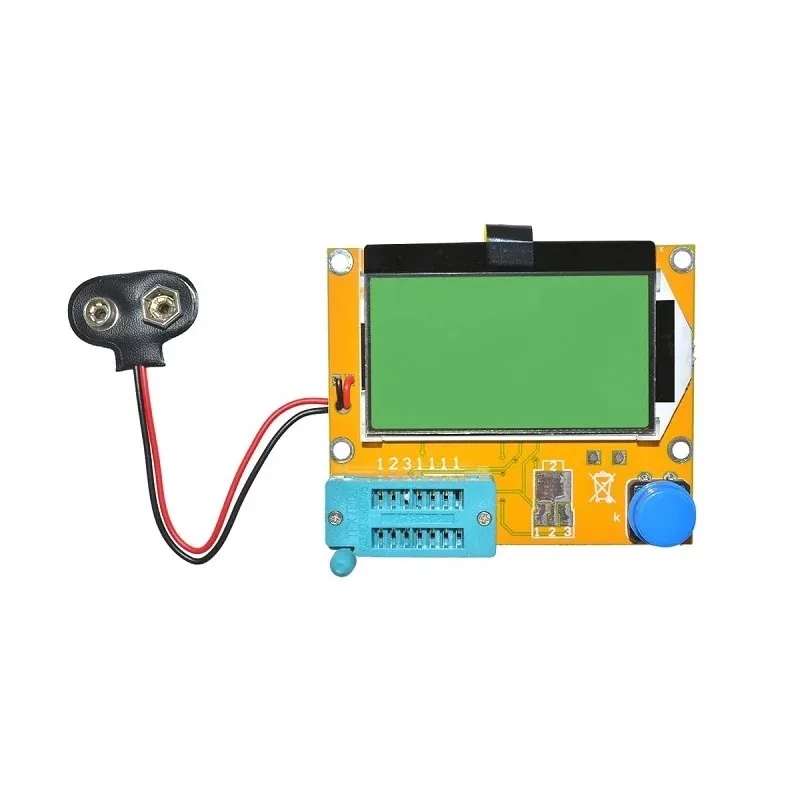
LCR-T4 Component Tester – Transistor, Resistance, Capacitance
Measure the actual β (hFE) of your BJT before using it in a circuit. This affordable tester identifies pinout and gain in seconds.
Frequently Asked Questions
What happens if a BJT is operated between the active and saturation regions?
This is called the quasi-saturation region. The transistor is partially on — VCE is reduced from the active region value but not yet at V_CE_sat. In analog circuits this is an operating point like any other. In switching circuits, it means the transistor is dissipating the product of both significant VCE and IC simultaneously — generating maximum heat. Avoid this in power switching by ensuring the transistor is either fully in saturation (ON) or fully in cutoff (OFF).
Why is VBE always approximately 0.7V?
It is the forward voltage of the base-emitter p-n junction, which follows the diode equation. For silicon, this is approximately 0.6V–0.7V at room temperature. It decreases by about 2mV/°C as temperature rises — an important consideration for thermally sensitive analog circuits.
Can I drive an inductive load (motor, relay) directly from a BC547?
Yes for relay coils (typically 50–100mA). Always add a flyback diode across the inductive load. For motors above a few hundred milliamperes, use a TIP120, TIP122, or a dedicated motor driver IC (L298N, DRV8833) instead.
How do I tell which leg is base, collector, and emitter on a TO-92 transistor?
With the flat side of the TO-92 package facing you and leads pointing down, for most common NPN transistors (BC547, 2N2222): left = Collector, centre = Base, right = Emitter. Always verify with the specific datasheet as some manufacturers differ.
What is the difference between a Darlington pair and a single BJT?
A Darlington pair connects two transistors so the emitter of the first drives the base of the second. The combined β is approximately β1 × β2, enabling very high current gain (1000+). This allows a weak signal to control several amps. The tradeoff is higher VCE_sat (~1.0–1.4V instead of 0.2V) and slower switching speed.
Conclusion
Mastering the three BJT regions of operation — cutoff, active, and saturation — is the foundation of all transistor circuit design. Cutoff gives you an open switch. Saturation gives you a closed switch. Active gives you an amplifier. Every circuit you build with a BJT exploits one or more of these states, and knowing which state you are targeting (and ensuring the biasing keeps you there) is the difference between a circuit that works and one that doesn’t.
Start with a simple relay driver using the BC547 or 2N2222 — it will immediately make all three regions tangible. Then move on to the common emitter amplifier, where you will feel the power of analog circuit design. Both components are available at Zbotic at genuinely affordable prices.


Add comment