
The astable multivibrator 555 timer circuit is arguably the most important and widely-taught circuit in all of electronics. This self-sustaining oscillator generates a continuous square wave output without any external trigger — making it the heartbeat of countless hobbyist projects, from simple LED blinkers to sophisticated motor speed controllers, tone generators, and clock sources for digital circuits. The NE555 timer IC, introduced by Signetics in 1972, remains the world’s best-selling analog IC to this day, and for good reason: it costs under ₹10, is nearly indestructible, and works beautifully across a huge range of supply voltages and frequencies.
Table of Contents
- Inside the 555 Timer: How It Works
- Astable Multivibrator Circuit Diagram
- Frequency and Duty Cycle Calculations
- Component Selection for Your Target Frequency
- 50% Duty Cycle and Variable Duty Cycle Tricks
- Practical Project Ideas
- 555 Variants: NE555, LM555, TLC555, CMOS 7555
- Frequently Asked Questions
Inside the 555 Timer: How It Works
To master the astable 555 timer circuit, it helps enormously to understand what’s happening inside the IC. The 555 contains three key internal blocks:
1. Resistor Voltage Divider: Three equal resistors (each 5kΩ, hence the name “555”) connected in series from VCC to GND. They create two reference voltages:
- Upper comparator threshold: 2/3 × VCC
- Lower comparator threshold: 1/3 × VCC
2. Two Comparators: One compares the THRESHOLD pin (pin 6) to 2/3 VCC. The other compares the TRIGGER pin (pin 2) to 1/3 VCC. Their outputs control the SR flip-flop.
3. SR Flip-Flop + Discharge Transistor: The flip-flop stores the current state (HIGH or LOW). Its Q-bar output drives the OUTPUT pin (pin 3) through an output stage. It also controls the DISCHARGE transistor (pin 7) — when the flip-flop output is HIGH, the discharge transistor is ON (shorting pin 7 to GND).
In astable mode, the timing capacitor alternately charges and discharges between 1/3 VCC and 2/3 VCC, toggling the flip-flop and creating the continuous square wave output.
Astable Multivibrator Circuit Diagram
The standard astable 555 timer circuit requires only 5 external components:
Component list:
- NE555 IC (DIP-8 package)
- R1: Resistor from VCC to PIN 7 (DISCHARGE)
- R2: Resistor from PIN 7 (DISCHARGE) to PIN 6/2 (THRESHOLD/TRIGGER)
- C1: Timing capacitor from PIN 6/2 to GND
- C2: 10nF or 100nF bypass capacitor from PIN 5 (CONTROL) to GND
Wiring connections:
- Pin 1 (GND) → GND rail
- Pin 2 (TRIGGER) → Pin 6 (THRESHOLD) — connect together, also to top of C1
- Pin 3 (OUTPUT) → your load (LED with resistor, speaker, relay, etc.)
- Pin 4 (RESET) → VCC (disable reset = always running)
- Pin 5 (CONTROL) → 10nF ceramic cap → GND (noise bypass)
- Pin 6 (THRESHOLD) → top of C1 (connected to Pin 2)
- Pin 7 (DISCHARGE) → junction of R1 and R2
- Pin 8 (VCC) → 5V to 15V power supply
- R1 connects VCC to Pin 7 (DISCHARGE)
- R2 connects Pin 7 to Pins 2/6
- C1 bottom → GND
Why the bypass cap on Pin 5? The internal voltage divider’s midpoint (Pin 5, CONTROL) is sensitive to noise. Without the 10nF bypass cap, power supply ripple couples into the comparator thresholds and causes jitter in the output frequency. Always include this cap — it costs less than ₹0.50 and makes a huge difference in circuit stability.

0.1µF Ceramic Capacitor (Pack of 50)
104 ceramic capacitors for 555 timer bypass and timing. Every 555 project needs these — pack of 50 so you’ll always have bypass caps on hand.
Frequency and Duty Cycle Calculations
The 555 astable circuit’s timing depends on how long C1 takes to charge and discharge between the two threshold voltages (1/3 VCC and 2/3 VCC). The formulas are:
Charge time (t_HIGH — time output is HIGH):
tH = 0.693 × (R1 + R2) × C1
Discharge time (t_LOW — time output is LOW):
tL = 0.693 × R2 × C1
Period (T — total cycle time):
T = tH + tL = 0.693 × (R1 + 2×R2) × C1
Frequency (f):
f = 1/T = 1.44 / ((R1 + 2×R2) × C1)
Duty cycle (D — fraction of time output is HIGH):
D = tH / T = (R1 + R2) / (R1 + 2×R2) × 100%
Note: In a standard astable 555 circuit, the duty cycle is always greater than 50% because R1 participates in charging but not discharging. The minimum duty cycle approaches 50% when R1 is very small compared to R2.
Worked example: R1 = 10kΩ, R2 = 100kΩ, C1 = 10µF
- tH = 0.693 × (10k + 100k) × 10µF = 0.693 × 110,000 × 0.000010 = 0.763 s
- tL = 0.693 × 100k × 10µF = 0.693 s
- T = 0.763 + 0.693 = 1.456 s
- f = 1 / 1.456 = 0.69 Hz (~1 blink per 1.5 seconds)
- Duty cycle = 110k / (10k + 200k) × 100% = 52.4%
Component Selection for Your Target Frequency
Use this quick reference table to select components for common target frequencies. These use R1 = 1kΩ to keep duty cycle close to 50%:
| Target Frequency | R1 | R2 | C1 | Application |
|---|---|---|---|---|
| 0.5 Hz | 1kΩ | 1MΩ | 1µF | Slow LED blinker |
| 1 Hz | 1kΩ | 680kΩ | 1µF | 1 second timer clock |
| 440 Hz | 1kΩ | 1.6kΩ | 1µF | Musical note A4 |
| 1 kHz | 1kΩ | 680Ω | 1µF | Audio test tone |
| 38 kHz | 1kΩ | 18kΩ | 1nF | IR remote carrier |
Pro tip: Replace R2 with a 10kΩ fixed resistor in series with a 100kΩ potentiometer to make frequency adjustable. This gives you a variable-frequency oscillator (VFO) — perfect for tone generators, motor controllers, and lab test equipment. Replace C1 with a rotary switch selecting different capacitor values for decade range switching.

1.5 Ohm [0.25W] 1/4W Metal Film Resistor MFR (Pack of 100)
Precision metal film resistors for accurate 555 timer frequency setting. Lower tolerance (1%) means your target frequency is more predictable than with carbon film.
50% Duty Cycle and Variable Duty Cycle Tricks
Standard astable 555 circuits always have duty cycle above 50%. Here’s how to break that limitation:
Method 1: Diode bypass for near-50% duty cycle
Add a 1N4148 diode in parallel with R2 (cathode toward pin 7, anode toward pins 2/6). During charging, current flows through R1+R2. During discharging, current flows through R1+diode (bypassing R2 for the discharge path). With small R1: tH ≈ 0.693 × R2 × C1, tL ≈ 0.693 × R1 × C1. If R1 = R2: 50% duty cycle. If R1 < R2: duty cycle < 50%!
Method 2: Output inversion for below-50%
Connect the load to pin 7 (DISCHARGE) through a pull-up resistor instead of pin 3 (OUTPUT). Pin 7 is HIGH (transistor OFF) when pin 3 is LOW, and vice versa. This inverts the output and effectively swaps tH and tL.
Method 3: Control voltage modulation
Applying a varying voltage to Pin 5 (CONTROL VOLTAGE) modulates the threshold voltages in real time, changing both frequency and duty cycle simultaneously. This is how the 555 can be used for VCO (voltage-controlled oscillator) applications — feed an audio signal to Pin 5 for frequency modulation (FM).
Practical Project Ideas
1. LED Police Flasher
Two 555 timers, one running fast (10Hz) and one slow (2Hz). The fast 555 drives the LED, and the slow 555 controls its enable pin. Result: the LED flashes rapidly in short bursts — exactly like emergency vehicle lights. Total cost: under ₹50.
2. PWM Motor Speed Controller
Set up a 555 astable at 1kHz with a potentiometer controlling R2. Feed the output through an N-channel MOSFET (IRFZ44N) to control a DC motor. The potentiometer adjusts duty cycle from ~50% to ~95%, giving smooth speed control. Add a flyback diode across the motor terminals for protection. This circuit can handle motors up to 10A at 12V — perfect for electric vehicles and automation projects.
3. Ultrasonic Distance Measurement Helper
Generate a 40kHz carrier frequency (R1=1kΩ, R2=18kΩ, C=1nF) to drive an ultrasonic transducer for DIY sonar ranging. Compare with the echo time on Arduino for distance calculation without relying on an HC-SR04 module.
4. Capacitance Meter
Configure the 555 as an astable and measure the output frequency. By solving the frequency formula for C (given fixed known R1 and R2), you can calculate unknown capacitor values. Build this into a handheld meter with an LCD frequency display — a useful lab instrument.

2N2222 NPN Transistor (Pack of 20)
General-purpose NPN transistors for amplifying the 555 timer output to drive heavier loads like relays, buzzers, and motor driver stages. Pack of 20.
555 Variants: NE555, LM555, TLC555, CMOS 7555
Not all 555s are created equal. Here’s how to choose the right variant for your project:
NE555 (bipolar, Signetics/Texas Instruments): The original. 5V to 15V supply, can source/sink 200mA on output. Strong output for direct relay driving. Can interfere with sensitive analog circuits due to internal current spikes. Best for 5V–12V projects where output current matters.
LM555 (bipolar, various manufacturers): Pin-compatible with NE555. Slightly improved specifications in some parameters. The most common substitute you’ll find in Indian markets at similar pricing.
CMOS 7555 / LMC555 / ICM7555: CMOS version. Supply from 2V to 15V, extremely low quiescent current (~60µA vs ~10mA for NE555). Output swing goes rail-to-rail (nearly 0V to VCC). Better for battery-powered projects, 3.3V systems, and precision timing where the NE555’s internal loading would affect results. Output current limited to ~100mA.
TLC555 (CMOS, Texas Instruments): High-performance CMOS variant, very stable timing, low power. Preferred for precision frequency generation and long-life battery applications.
For most Indian maker projects at 5V or 9V, the NE555 or LM555 is perfect and costs ₹8–₹15. Use the 7555 when working with 3.3V systems, coin cell batteries, or when you need ultra-low power consumption.
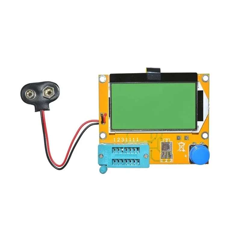
9V Battery Operated LCR-T4 LCD Graphical Transistor Tester
Measure resistors, capacitors, inductors, transistors, and MOSFETs automatically. Essential for verifying your 555 timer timing components and checking component values before building.
Frequently Asked Questions
Q: Why is my 555 timer getting hot?
The NE555 consumes about 10mA quiescent current even with no load, which generates ~50mW at 5V — warm but not dangerously hot. If it’s getting very hot, check for short circuits on the output, incorrect supply voltage (above 15V destroys the NE555), or wrong polarity. Also ensure C1 has correct polarity if using an electrolytic capacitor — reversed polarity causes capacitor heating, not IC heating.
Q: My 555 frequency is way off from calculation — why?
Electrolytic capacitors have ±20% tolerance, and resistors typically ±5%. Combined tolerances can give ±30% frequency error. For precision, use film capacitors (polypropylene or polyester) with ±5% or better tolerance. Also measure your actual resistor and capacitor values with a multimeter or LCR meter and recalculate — don’t trust the printed value alone.
Q: Can I use the 555 timer as a PWM controller for LED brightness?
Yes — this is one of the most popular 555 applications. Set the frequency well above 50Hz (use 1kHz to avoid visible flicker). Connect the output through a current-limiting resistor to the LED. Adjust the duty cycle with a potentiometer. For higher-power LEDs, add an NPN transistor (BC547 for small LEDs, 2N2222 for higher current) between the 555 output and the LED.
Q: What is the maximum frequency a 555 timer can generate?
The NE555 datasheet specifies maximum operating frequency of ~500kHz, with practical reliable operation up to ~200kHz. Above that, propagation delays and internal switching times degrade the output. The CMOS 7555 can reach ~2MHz. For higher frequencies, use dedicated oscillator ICs, crystal oscillators, or microcontroller PWM outputs.
Q: Can I run the 555 timer from a 3.7V LiPo battery?
The standard NE555/LM555 requires a minimum of 4.5V, so it won’t work reliably from a single LiPo cell at 3.7V nominal. Use the CMOS 7555 (ICM7555 or LMC555), which operates from 2V to 15V. Alternatively, use a boost converter to raise the LiPo voltage to 5V, then power the NE555 normally.
Start building your 555 timer projects today! Get resistors, capacitors, transistors, and all the components you need from Zbotic Electronics Basics. Genuine components, competitive prices, and fast delivery across India. Your next circuit is just a few clicks away!


Add comment