
A bidirectional logic level converter is the go-to solution for connecting mixed-voltage devices in any maker project. Unlike one-way resistor dividers, a bidirectional converter handles signals flowing in both directions on the same wire — which is exactly what I²C and SPI need. Whether you are connecting an ESP32 (3.3V) to a 5V LCD, wiring a Raspberry Pi to a 5V sensor cluster, or building a professional IoT device, understanding how these converters work will save you hours of debugging and prevent permanent hardware damage.
How a Bidirectional Level Converter Works
The most common bidirectional level converter circuit uses an N-channel MOSFET (typically BSS138 in SMD or 2N7000 in through-hole). The elegance of this circuit is that it handles signal flow in both directions without any direction control pin — it is truly automatic.
The key insight is that N-channel MOSFETs have a body diode that conducts in the reverse direction (from source to drain) when forward biased. This, combined with the MOSFET’s switching action, creates a circuit that allows signals to pass in both directions between a low-voltage rail (LV: 1.8V–3.3V) and a high-voltage rail (HV: 3.3V–5V).
This circuit was originally described in Philips Semiconductor Application Note AN10441 (2003) for I²C voltage translation, and it remains the most widely used approach for open-drain bidirectional signals 20+ years later.
The BSS138 MOSFET Circuit: Deep Dive
Understanding this circuit deeply helps you build it from discrete components when modules are not available and helps you diagnose problems when signals misbehave.
The Full Circuit for One Channel
LV (e.g., 3.3V) ─────[R_LV 10kΩ pull-up]─────┬──── Source (MOSFET)
                                                 │           │
                                                 │       Gate ← LV rail (3.3V)
3.3V Device IO ──────────────────────────────────┘       │
                                                     Drain ────[R_HV 10kΩ pull-up]──── HV (5V)
                                                         │
                                                    5V Device IO
State 1: Both sides idle (no device pulling LOW)
Both sides float HIGH — the 3.3V side is pulled to LV (3.3V) through R_LV, and the 5V side is pulled to HV (5V) through R_HV. The MOSFET Gate is at 3.3V, Source is at 3.3V, so Vgs = 0V — the MOSFET is OFF. The bus idles at their respective HIGH levels.
State 2: 3.3V device pulls low
The 3.3V device’s open-drain output pulls its IO pin to GND. The Source of the MOSFET is now pulled to GND. Gate is still at 3.3V. Vgs = 3.3V — exceeds Vth (typically 0.8–1.5V for BSS138), MOSFET turns ON. The Drain is now connected through the MOSFET to Source (GND), pulling the 5V side LOW too. The 5V device sees a LOW — correct signal transmission.
State 3: 5V device pulls low
The 5V device pulls its IO to GND. This pulls the Drain to GND. The Body diode of the MOSFET (Source-to-Drain) conducts in the forward direction when Drain is below Source by >0.7V — current flows through the body diode, pulling the Source (and thus the 3.3V device’s IO) to approximately 0.7V (one diode drop above drain). This is close enough to GND to register as a valid LOW on the 3.3V device. Simultaneously, as the Source voltage drops toward 0V, Vgs increases and the MOSFET turns on more fully, pulling the source cleanly to near-zero. The 3.3V device sees a LOW — correct bidirectional signal.
Speed and Capacitance
The pull-up resistors and MOSFET gate capacitance form an RC filter. The time constant τ = R × C determines maximum speed. For 10 kΩ pull-ups and typical MOSFET gate capacitance of ~5 pF, τ ≈ 50 ns — limiting signals to about 1–2 MHz. For I²C at 400 kHz, this is fine. For SPI at 8 MHz+, you need lower pull-up values (1 kΩ) or a dedicated IC.
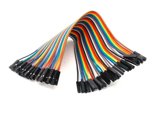
10CM Female to Female Breadboard Jumper Wires — 40 Pcs
Connect level converter modules to your microcontroller and sensors cleanly. Colour-coded for easy identification of I2C and SPI signal lines.
Wiring for I²C: SDA and SCL Shifting
I²C uses two open-drain, bidirectional lines: SDA (data) and SCL (clock). Both require pull-up resistors to the supply voltage on each side. A bidirectional MOSFET converter is the correct choice.
Step-by-Step Wiring for a 4-Channel Module
- LV pin → 3.3V from your microcontroller (ESP32, STM32, Raspberry Pi)
- HV pin → 5V from your 5V power supply or Arduino 5V pin
- GND → Common ground (connect ALL GNDs together — this is crucial)
- LV1 → ESP32 SDA
- LV2 → ESP32 SCL
- HV1 → 5V Sensor/Device SDA
- HV2 → 5V Sensor/Device SCL
Pull-Up Resistors with Modules
Most BSS138 modules include onboard 10 kΩ pull-ups on both LV and HV sides for each channel. This means you may NOT need additional external pull-ups. However, if you already have pull-ups on your sensor board or MCU breakout, the parallel combination can reduce the effective pull-up resistance too much. Check with a multimeter: measure resistance from SDA to VCC with all pull-ups active. Aim for 4.7 kΩ at 100 kHz, 2.2 kΩ at 400 kHz.
Multiple I²C Devices on the Shifted Bus
You can connect multiple 5V I²C devices on the HV side of the converter — they all share the same SDA/SCL bus. Each device needs a unique I²C address. The converter handles all of them simultaneously since it is simply part of the shared bus. Ensure the combined pull-up strength is appropriate for the number of devices (add capacitance from all device inputs).

1.3 Inch I2C/IIC 128×64 OLED Display Module — 4 Pin
A popular I2C device to use with your level converter. This OLED works at 3.3V and 5V, making it a great test device for level shifting experiments.
Wiring for SPI: MOSI, MISO, SCK, and CS
SPI is more complex than I²C because it has more signals, and critically, it is a push-pull (not open-drain) protocol. The BSS138 MOSFET circuit is designed for open-drain signals. This matters:
- SCK (clock): Unidirectional from master to slave. A resistor divider (for 5V→3.3V) or the MOSFET circuit (slightly limited by push-pull) works.
- MOSI (master out, slave in): Unidirectional. Same as SCK.
- MISO (master in, slave out): Unidirectional from slave to master. If slave is 5V, a resistor divider protects the 3.3V master.
- CS/SS: Unidirectional from master to slave.
The Problem with Push-Pull and MOSFET Converters
When the 5V device actively drives MOSI HIGH (push-pull), the BSS138 source sees 5V — but gate is at 3.3V, so Vgs is negative and the MOSFET is OFF. The 3.3V side is isolated. In practice this means the 3.3V side does not see the HIGH signal at all. For true bidirectional push-pull SPI level shifting, use:
- TXB0108 IC (Texas Instruments): Push-pull compatible, auto-direction sensing, up to 100 Mbps
- 74LVC125 or 74LVC245: Manual direction control (DIR pin), high speed
- Separate unidirectional channels: Resistor divider for 5V→3.3V lines, direct connection or BJT for 3.3V→5V lines
Practical SPI Wiring at Slow Speeds (<1 MHz)
For SPI at low speeds (Arduino talking to a 5V display at 500 kHz), the MOSFET module often works acceptably even for push-pull SPI due to the pull-up resistors providing a quasi-open-drain environment. Test it — if it works reliably, fine. If you see corruption, switch to the TXB0108 or dedicated per-direction solutions.
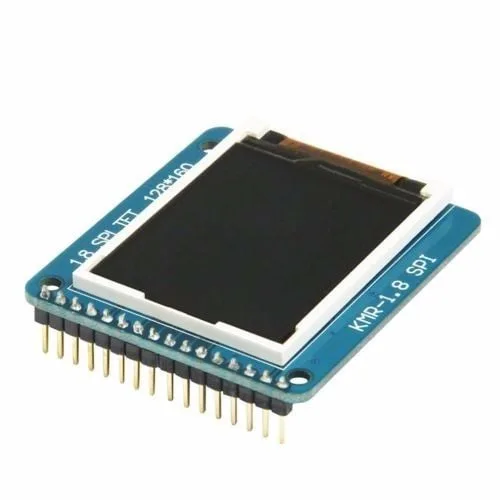
1.8 Inch SPI 128×160 TFT LCD Display for Arduino
A classic SPI display module to practice level shifting with. This display uses SPI protocol and works well with both 3.3V and 5V microcontrollers via a level converter.
Ready-Made Level Converter Modules: What is Inside
The popular 4-channel (and 8-channel) bidirectional logic level converter modules sold online contain:
- 4× BSS138 N-channel MOSFET (SOT-23 SMD package)
- 8× 10 kΩ SMD resistors (pull-ups, two per channel)
- Two sets of header pins (LV side and HV side)
- LV, HV, and two GND pins
These modules cost ₹40–₹80 at Indian online stores. They are produced in enormous volumes and are generally reliable — the BSS138 is a well-characterised part with consistent parameters. The main variance between suppliers is PCB quality and soldering quality; check that all pads are cleanly soldered if you source very cheap ones from unknown suppliers.
Module Pinout (Standard 4-Channel)
| Pin | Description |
|---|---|
| LV | Low voltage supply (1.8V–3.3V) |
| HV | High voltage supply (3.3V–5V) |
| GND (×2) | Common ground — connect both to system GND |
| LV1–LV4 | Low-voltage side signal pins (connect to 3.3V MCU) |
| HV1–HV4 | High-voltage side signal pins (connect to 5V device) |
Troubleshooting Common Level Converter Problems
Problem: Signal stuck LOW on one side
Cause: Missing or wrong pull-up resistors. The MOSFET circuit requires pull-ups on BOTH sides to function. Without them, the bus cannot go HIGH.
Fix: Add 4.7–10 kΩ resistors from each signal pin to the respective LV or HV rail.
Problem: I²C communication works sometimes but is unreliable
Cause: Pull-up resistance too high (too weak a pull-up). Multiple modules or devices each contributing pull-ups may create too-strong combined pull-ups after you add more devices, or individual pull-ups that are too weak for bus capacitance.
Fix: Measure the effective pull-up resistance with a multimeter (resistance from SDA to VCC with all devices connected but powered off). Target 2.2–4.7 kΩ for 400 kHz I²C.
Problem: SPI data corruption at higher speeds
Cause: MOSFET circuit RC time constant too slow for push-pull SPI at 4 MHz+.
Fix: Lower pull-up resistors to 2.2 kΩ or 1 kΩ, or switch to TXB0108 IC.
Problem: 3.3V device damaged after connecting to converter
Cause: Common ground not connected. Without a common ground, the LV and HV grounds float relative to each other, causing undefined voltages.
Fix: Always connect GND of ALL devices (3.3V MCU, converter module, 5V device) together to a single common ground point.
Problem: No signal passing at all
Cause: LV and HV power pins not connected or swapped.
Fix: Verify with a multimeter: LV should measure 3.3V to GND, HV should measure 5V to GND. Module orientation matters — LV side pins should connect to the 3.3V device side only.

10CM Male to Male Breadboard Jumper Wires — 40 Pcs
Neatly route level converter signals on your breadboard. Colour-code your 3.3V and 5V signal lines to avoid mix-ups while prototyping.
When to Use a Dedicated IC Instead
The BSS138 MOSFET circuit is excellent but not perfect for every application. Here are the situations where you should reach for a dedicated translator IC:
- SPI at >4 MHz: Use TXB0108 or 74LVC245. The MOSFET circuit cannot keep up reliably above 2–3 MHz.
- Unidirectional parallel buses (8-bit data bus): 74LVC245 or 74LVC244 handle 8 channels in one package with a DIR control pin.
- Very low voltage (1.2V, 1.8V) to 3.3V: MOSFET Vth may not be exceeded reliably at 1.2V. Use dedicated low-voltage translators like TXB0104 with correct voltage ranges.
- High reliability / commercial product: Dedicated ICs have characterised specs, known propagation delays, and are better suited for production designs than discrete MOSFET circuits.
- I²C at 1 MHz (fast-plus mode): Use PCA9306 or similar — the MOSFET circuit introduces too much capacitance for fast-plus speeds.
Frequently Asked Questions
Q1: Can I use the same bidirectional converter for UART?
Yes, the MOSFET converter works for UART, but UART is push-pull (not open-drain). At typical UART speeds (up to 115200 baud = ~115 kHz effective signal rate), the MOSFET pull-ups can follow the signal edges adequately. For UART at >1 Mbps, the pull-ups may not be fast enough and a dedicated IC would be more reliable.
Q2: Do I need a level converter if my 3.3V MCU has 5V-tolerant GPIO?
For receiving 5V signals — no, 5V-tolerant pins can accept 5V inputs directly. But you still need level shifting if you need the 5V device to reliably detect the 3.3V output as a HIGH signal (CMOS 5V threshold ~3.5V means 3.3V may not always register as HIGH). Check the 5V device’s VIH specification.
Q3: How many devices can I connect on one I²C channel through the level converter?
There is no hard limit from the converter itself — it is just part of the I²C bus. The I²C specification limits total bus capacitance to 400 pF for standard pull-up values. Each device adds ~5–50 pF. Practically, 5–10 devices is usually fine on a short PCB; long cables with many devices may require I²C repeaters or bus buffers.
Q4: Can I run the level converter from 3.3V and 5V on the same USB power?
Yes, as long as the 5V rail comes from a regulated 5V source (e.g., Arduino Uno’s 5V pin, a USB power module, or an SMPS output). The GND must be common between all rails. Avoid powering the HV rail from a different USB charger than the LV rail — floating grounds cause unreliable operation and can damage components.
Q5: My level converter module gets warm during use. Is this normal?
A slight warmth is normal if the pull-up resistors are conducting continuously (e.g., bus lines held LOW for extended periods). Each 10 kΩ pull-up to 5V with line at GND dissipates 5V²/10kΩ = 2.5 mW — negligible. If the module is noticeably hot, check for a short or an incorrect connection causing continuous high current flow. The BSS138 in normal operation stays well under 60°C.
Shop Zbotic for transistors, resistors, display modules, jumper wires, and all the components you need to prototype level-shifting circuits — fast delivery across India.


Add comment