Zbotic Logo Zbotic Logo
  • Home
  • Shop
  • Sale
  • 3D Print Service
  • PCB Service
  • B2B
  • Blogs
  • Contact Us
0 0

View Wishlist Add all to cart

0 0
0 Shopping Cart
Shopping cart (0)
Subtotal: ₹0.00

View cartCheckout

  • Shop
  • About Us
  • Contact Us
  • Reseller
  • Blogs
020 69134444
1800 209 0998
[email protected]
Help Desk
Facebook Twitter Instagram Linkedin YouTube
Zbotic Logo Zbotic Logo
0 0

View Wishlist Add all to cart

0 0
0 Shopping Cart
Shopping cart (0)
Subtotal: ₹0.00

View cartCheckout

All departments
  • 3D Print Service
  • 3D Printer
  • Batteries & Chargers
  • Development Boards
  • Drone Parts
  • EBike parts
  • Sensor Modules
  • Electronic Components
  • Electronic Modules
  • IoT and Wireless
  • Mechanical Parts and Workbench Tools
  • Motors & Drivers & Pumps & Actuators
  • DIY and Robot Kits
  • Show more
  • Home
  • Shop
  • Sale
  • 3D Print Service
  • PCB Service
  • B2B
  • Blogs
  • Contact Us
Return to previous page
Home Arduino & Microcontrollers

PCB Technical Design Guidelines

PCB Technical Design Guidelines

March 17, 2026 /Posted by

PCB Design Guidelines

Impedance Control

Controlled impedance is available for high-speed digital and RF designs. Use the impedance calculator when ordering to specify your target impedance, trace width, and dielectric thickness.

PCB design and manufacturing guidelines

Panelization Guidelines

  • V-Cut: For rectangular boards only. Minimum board thickness: 0.6mm
  • Tab routing: For irregular shapes. Minimum 3 tabs per board
  • Stamp holes: 0.5mm holes with 0.75mm spacing between them
  • Panel rails: minimum 5mm width recommended
  • Fiducial marks: 1mm diameter, 2mm clearance from edge

BGA Design Recommendations

  • Use NSMD (Non-Solder Mask Defined) pads for better solder joint reliability
  • Via-in-pad: use filled and capped vias to prevent solder wicking
  • Minimum pad pitch: 0.4mm (requires 4+ layer boards)
  • Add test points for boundary scan testing

Minimum Design Rules

Parameter 1-2 Layer 4+ Layer
Min trace width 0.127mm (5mil) 0.1mm (3.94mil)
Min spacing 0.127mm (5mil) 0.1mm (3.94mil)
Min via diameter 0.3mm 0.2mm
Min via drill 0.15mm 0.15mm
Min annular ring 0.13mm 0.1mm
Min solder mask bridge 0.2mm 0.1mm

Edge Plating

Include edge plating requirements in your Gerber file as copper on the board edge. Add a picture and note in remarks: “Edge plating required.”

Panelization with different designs

Aluminum Substrate Notes

  • White and black silkscreen supported
  • White silkscreen on green/black solder mask; black on white solder mask
  • Silkscreen on bare aluminum not recommended (poor adhesion)

Countersink Holes

Countersink holes are supported. Specify the hole diameter, countersink diameter, and angle in your design files or remarks.
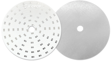
Aluminum PCB

Aluminum PCB
Metal core PCBs

Metal core PCBs

Preventing Breakage

For boards with narrow sections (< 2mm width), add support rails or panelize to prevent breakage during manufacturing and shipping.

Share Post
  • Facebook
  • Linkedin
  • Whatsapp
PCB Capabilities & Specifi...
pcb help 608699
pcb help 608701
Stencil Ordering Guide

Related posts

Svg%3E
Read more

Arduino Batch Programming: Flash Multiple Boards Quickly

April 1, 2026 0
Table of Contents Introduction Components and Hardware Setup Wiring Diagram and Connections Complete Code with Explanation Customization and Improvements Troubleshooting... Continue reading
Svg%3E
Read more

Arduino Based Radar System with Ultrasonic Sensor

April 1, 2026 0
Table of Contents Introduction Components and Hardware Setup Wiring Diagram and Connections Complete Code with Explanation Customization and Improvements Troubleshooting... Continue reading
Svg%3E
Read more

Arduino Automatic Plant Monitor: Sunlight, Moisture, Temperature

April 1, 2026 0
Table of Contents Introduction Components and Hardware Setup Wiring Diagram and Connections Complete Code with Explanation Customization and Improvements Troubleshooting... Continue reading
Svg%3E
Read more

Arduino Lie Detector: GSR Sensor Polygraph Project

April 1, 2026 0
Table of Contents Introduction Components and Hardware Setup Wiring Diagram and Connections Complete Code with Explanation Customization and Improvements Troubleshooting... Continue reading
Svg%3E
Read more

Arduino Metal Detector: Build a Treasure Finder

April 1, 2026 0
Table of Contents Introduction Components and Hardware Setup Wiring Diagram and Connections Complete Code with Explanation Customization and Improvements Troubleshooting... Continue reading

Comments are closed

Facebook Twitter Instagram Pinterest Linkedin Youtube

Get the latest deals and more.

Download on Google Play Download on the App Store

Call us: 020 69134444 / 1800 209 0998

Monday - Saturday 09:30 AM - 06:00 PM
For Technical Supports Email: [email protected]
For Sales / Enquiries Email: [email protected]

  • My Account

    • Cart

    • Wishlist

    • Checkout

    • My Orders

    • Track Order

    • My Account

  • Information

    • FAQs

    • Blogs

    • Career

    • About Us

    • Contact Us

    • Payment Options

  • Policies

    • Privacy Policy

    • Terms & Conditions

    • GST Input Tax Credit

    • Shipping Return Policy

    • E-Waste Collection Points

    • Our Sitemap

© Zbotic.in is registered trademark of Moxie Supply Pvt Ltd – All Rights Reserved
Login
Use Phone Number
Use Email Address
Not a member yet? Register Now
Reset Password
Use Phone Number
Use Email Address
Register
Already a member? Login Now