Zbotic Logo Zbotic Logo
  • Home
  • Shop
  • Sale
  • 3D Print Service
  • PCB Service
  • B2B
  • Blogs
  • Contact Us
0 0

View Wishlist Add all to cart

0 0
0 Shopping Cart
Shopping cart (0)
Subtotal: ₹0.00

View cartCheckout

  • Shop
  • About Us
  • Contact Us
  • Reseller
  • Blogs
020 69134444
1800 209 0998
[email protected]
Help Desk
Facebook Twitter Instagram Linkedin YouTube
Zbotic Logo Zbotic Logo
0 0

View Wishlist Add all to cart

0 0
0 Shopping Cart
Shopping cart (0)
Subtotal: ₹0.00

View cartCheckout

All departments
  • 3D Print Service
  • 3D Printer
  • Batteries & Chargers
  • Development Boards
  • Drone Parts
  • EBike parts
  • Sensor Modules
  • Electronic Components
  • Electronic Modules
  • IoT and Wireless
  • Mechanical Parts and Workbench Tools
  • Motors & Drivers & Pumps & Actuators
  • DIY and Robot Kits
  • Show more
  • Home
  • Shop
  • Sale
  • 3D Print Service
  • PCB Service
  • B2B
  • Blogs
  • Contact Us
Return to previous page
Home Arduino & Microcontrollers

PCB & Stencil Ordering Instructions

PCB & Stencil Ordering Instructions

March 17, 2026 /Posted by

Instructions for PCB Orders

1. Solder-Resistance Bridges

For solder-resistance bridges, spacing between pads/pins requires at least 0.2mm on 1-2 layer boards and 0.1mm on multilayer boards. Please add a note like “solder mask bridge is required” when ordering.

2. File Format Priority

Only Gerber files are processed. English descriptions, PDFs, DXF, Excel, and other non-Gerber files in your ZIP will be disregarded. If both PCB files and Gerber files exist, the Gerber file takes precedence.

3. Plated Slots

Minimum plated slot width is 0.5mm, with length at least twice the width. Rectangular slots without rounded corners are unsupported. For edge plating, include a picture in the Gerber file and mention it in remarks.

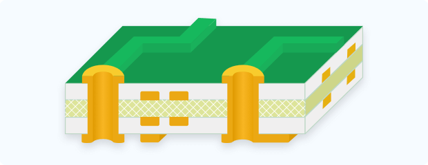
4. Board Outline & Slots

V-cut lines, cutouts, millings and slots must be in the same layer as the board outline. If not in the same layer, they will be missed. Design thickness of 0.15mm is recommended for outlines.

5. Silkscreen / Text Requirements

  • Minimum text width: 0.15mm
  • Minimum text height: 1mm
  • Preferred width-to-height ratio: 1:6
  • Outline fonts with filled lines need 0.15mm minimum line width
  • When silkscreen overlaps with solder mask openings, openings take priority

6. Multi-Layer PCBs

Three-layer PCBs are not manufactured. If you need an odd inner layer, it will be processed as the next even layer count (e.g., 3 layers → 4 layers).

PCB layer stack-up options

7. Panelization

We support V-cut panelization for rectangular and round shapes only. If self-panelized but ordered as “Single PCB,” the number of unique designs must not exceed 5. For “Panel by Customer,” designs must not exceed 10.

PCB panelization and different designs

8. Small Boards (≤50mm × 50mm)

Milling small boards perfectly is challenging. We recommend panelizing small boards for better results and handling.

9. Solder Mask Layer

The solder mask layer is a required layer. If absent or blank, the board defaults to full solder mask coverage. Design your solder mask openings correctly.

10. Remarks Field

A remark field exists for important information, but orders with English notes may take longer processing time. Use this sparingly.

11. Gerber Preview

The website preview is only for quick review before payment. It may not display your design exactly as intended — always verify your files independently.

Instructions for Stencil Orders

1. Solder Paste Layer

The stencil is made based on the paste layer. Ensure it contains all required elements. To avoid questions about differences between solder mask and paste layers, add a remark: “Please follow the solder paste layer only.”

SMT stencil manufacturing

2. Aperture Processing

IC, BGA, and 0805+ capacitor/resistor footprints are processed with standard aperture reduction by default. For exact paste layer matching, leave a remark requesting exact matching.

3. Stencil Thickness

Standard free thicknesses: 0.1, 0.12, 0.15, 0.18, 0.2mm. Special thicknesses (0.03-0.5mm) are available at additional cost.

4. Valid Area

For frame stencils, the valid area is within the adhesive tape. For non-frame stencils, approximately 8mm on each side is excluded for clamping.

5. Fiducials

Select “Etched Through” or “Etched Half” and include fiducial designs in your paste layer file.

6. Top+Bottom on Single Stencil

This option requires the stencil valid area to be larger than double the PCB size. Ensure your selected stencil size is large enough.

7. Packaging

  • Non-frame stencils under 25×25cm: plastic bags then flight cases
  • Over 25×25cm: wood plates and cardboard boxes
  • Frame stencils: cardboard boxes with wood plate protection
Share Post
  • Facebook
  • Linkedin
  • Whatsapp
Budget Home CCTV Setup Under 5...
blog budget home cctv setup under 5000 rupees india guide 599889
pcb help 608698
PCB Files Preparation Guide

Related posts

Svg%3E
Read more

Arduino Batch Programming: Flash Multiple Boards Quickly

April 1, 2026 0
Table of Contents Introduction Components and Hardware Setup Wiring Diagram and Connections Complete Code with Explanation Customization and Improvements Troubleshooting... Continue reading
Svg%3E
Read more

Arduino Based Radar System with Ultrasonic Sensor

April 1, 2026 0
Table of Contents Introduction Components and Hardware Setup Wiring Diagram and Connections Complete Code with Explanation Customization and Improvements Troubleshooting... Continue reading
Svg%3E
Read more

Arduino Automatic Plant Monitor: Sunlight, Moisture, Temperature

April 1, 2026 0
Table of Contents Introduction Components and Hardware Setup Wiring Diagram and Connections Complete Code with Explanation Customization and Improvements Troubleshooting... Continue reading
Svg%3E
Read more

Arduino Lie Detector: GSR Sensor Polygraph Project

April 1, 2026 0
Table of Contents Introduction Components and Hardware Setup Wiring Diagram and Connections Complete Code with Explanation Customization and Improvements Troubleshooting... Continue reading
Svg%3E
Read more

Arduino Metal Detector: Build a Treasure Finder

April 1, 2026 0
Table of Contents Introduction Components and Hardware Setup Wiring Diagram and Connections Complete Code with Explanation Customization and Improvements Troubleshooting... Continue reading

Comments are closed

Facebook Twitter Instagram Pinterest Linkedin Youtube

Get the latest deals and more.

Download on Google Play Download on the App Store

Call us: 020 69134444 / 1800 209 0998

Monday - Saturday 09:30 AM - 06:00 PM
For Technical Supports Email: [email protected]
For Sales / Enquiries Email: [email protected]

  • My Account

    • Cart

    • Wishlist

    • Checkout

    • My Orders

    • Track Order

    • My Account

  • Information

    • FAQs

    • Blogs

    • Career

    • About Us

    • Contact Us

    • Payment Options

  • Policies

    • Privacy Policy

    • Terms & Conditions

    • GST Input Tax Credit

    • Shipping Return Policy

    • E-Waste Collection Points

    • Our Sitemap

© Zbotic.in is registered trademark of Moxie Supply Pvt Ltd – All Rights Reserved
Login
Use Phone Number
Use Email Address
Not a member yet? Register Now
Reset Password
Use Phone Number
Use Email Address
Register
Already a member? Login Now