
PCB Trace Width Calculator: Current Capacity and Heat Management
One of the most critical — and most overlooked — aspects of PCB design is getting your trace widths right. If you search for a PCB trace width calculator for current capacity and heat, you will find dozens of online tools, but understanding the underlying principles separates a good PCB designer from a great one. An under-width trace can overheat, melt solder mask, and eventually open-circuit under load. An over-width trace wastes board real estate and increases manufacturing cost. This guide walks you through the IPC-2221 standard calculations, practical rules of thumb, and thermal management strategies used by professional PCB engineers across India and worldwide.
Why Trace Width Matters
A PCB trace is essentially a thin ribbon of copper on an insulating substrate (usually FR4). Like any conductor, it has resistance proportional to its length and inversely proportional to its cross-sectional area. When current flows, the trace dissipates power as heat (P = I² × R). Too much heat causes:
- Solder mask delamination and blistering
- FR4 substrate degradation (glass transition temperature Tg is typically 130–170°C for standard FR4)
- Trace resistance increase, leading to voltage drops that affect circuit performance
- In extreme cases, trace burnout and open circuit
- Nearby component damage from localised heat concentration
For most signal traces carrying microamperes to a few milliamperes, the minimum manufacturable width (typically 6 mil / 0.15 mm for standard PCB fabs) is more than adequate. The trace width calculation becomes critical for power traces carrying hundreds of milliamperes to tens of amperes.
IPC-2221 Standard and the Calculation Formula
The IPC-2221 standard (“Generic Standard on Printed Board Design”) provides the industry reference for trace width calculations. The fundamental relationship used in most trace width calculators is derived from empirical data collected over decades:
I = k × ΔT0.44 × A0.725
Where:
- I = Maximum current in amperes
- k = 0.048 for external traces (exposed to air), 0.024 for internal traces (buried in PCB stack)
- ΔT = Allowable temperature rise above ambient in °C (typically 10°C for conservative design, 20–30°C for less critical applications)
- A = Cross-sectional area of the trace in square mils (mil² = 0.001 inch squared)
Cross-sectional area: A = Width (mils) × Thickness (mils)
Standard copper weights and their thickness:
- 0.5 oz copper = 0.7 mil (17.5 µm) thick
- 1 oz copper = 1.4 mils (35 µm) thick — most common
- 2 oz copper = 2.8 mils (70 µm) thick
- 3 oz copper = 4.2 mils (105 µm) thick
Rearranged to solve for width:
First, solve for area: A = (I / (k × ΔT0.44))1/0.725
Then: Width (mils) = A / Thickness (mils)
Worked Example
You need an external trace to carry 3 A on a standard 1 oz PCB, allowing ΔT = 10°C:
- k = 0.048 (external), ΔT = 10°C, 100.44 ≈ 2.754
- A = (3 / (0.048 × 2.754))1/0.725 = (3 / 0.1322)1.379 = (22.69)1.379 ≈ 106 mil²
- Copper thickness = 1.4 mils (1 oz)
- Width = 106 / 1.4 ≈ 75.7 mils ≈ 1.92 mm
Round up to 2 mm for a conservative design. Most PCB designers add 20–25% safety margin, especially for high-reliability or industrial applications.
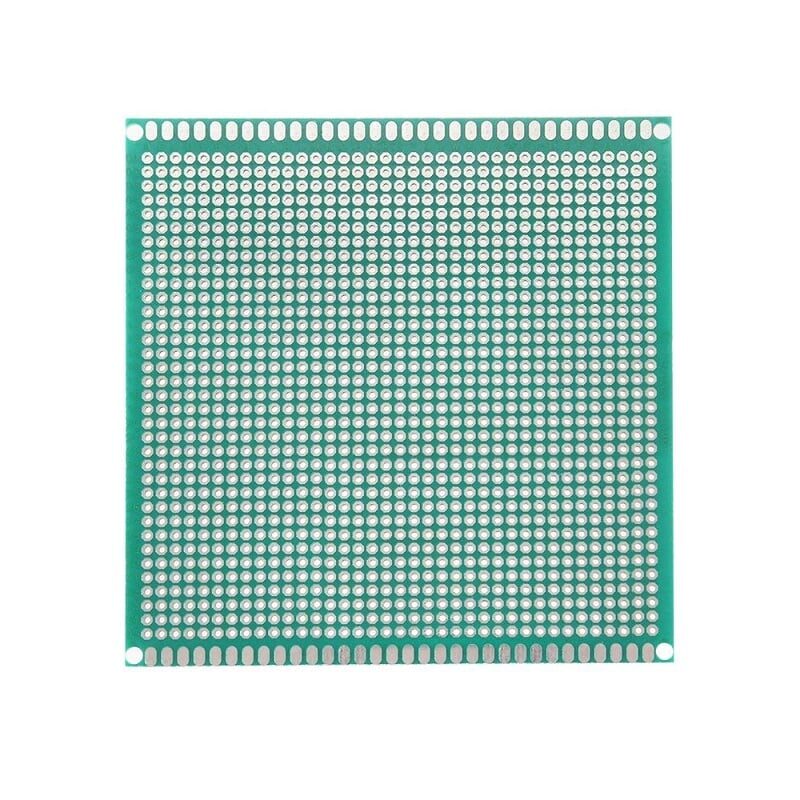
10×10 cm Universal PCB Prototype Board – Single Sided
Single-sided prototype board with 2.54 mm pitch. Ideal for hand-wiring high-current circuits while you verify your trace width calculations before committing to a custom PCB.
Internal vs External Traces
External traces (on the top or bottom layer of a PCB) can dissipate heat to the surrounding air by convection. Internal traces (on inner layers of a multilayer PCB) are surrounded by FR4 substrate, which has very poor thermal conductivity (approximately 0.3 W/m·K). This is why the IPC-2221 k-factor for internal traces is half that of external traces — an internal trace must be twice as wide as an external trace for the same current and temperature rise.
For a 4-layer PCB with a power plane on layer 2 and a ground plane on layer 3, power traces on the inner layers should always be wider than their external equivalents, or better yet, converted into partial fills and copper pours to maximise cross-sectional area.
Quick Reference: Trace Width vs Current Table
Based on IPC-2221, 1 oz copper, 10°C temperature rise above 25°C ambient:
| Current (A) | External Trace Width | Internal Trace Width | Resistance (mΩ/cm) |
|---|---|---|---|
| 0.3 A | 0.2 mm (8 mil) | 0.4 mm | 24.6 |
| 0.5 A | 0.35 mm (14 mil) | 0.7 mm | 14.1 |
| 1 A | 0.6 mm (24 mil) | 1.2 mm | 8.2 |
| 2 A | 1.1 mm (43 mil) | 2.2 mm | 4.5 |
| 3 A | 1.9 mm (75 mil) | 3.8 mm | 2.6 |
| 5 A | 2.9 mm (114 mil) | 5.8 mm | 1.7 |
| 10 A | 5.5 mm (216 mil) | 11 mm | 0.9 |
Note: For India’s tropical climate (ambient temperatures often 30–40°C), use ΔT = 10°C (total 40–50°C), which is stricter and accounts for the warmer baseline. Reduce the current rating by about 20% compared to table values if your PCB will see sustained 40°C ambient.
Thermal Management: Vias, Planes, and Copper Pours
Copper pours (polygon fills): For high-current paths, use a copper pour on one or more layers rather than a narrow trace. A copper pour connecting two high-current points has near-zero resistance along its perimeter and excellent heat spreading. In EasyEDA, KiCad, or Altium, right-click the net and add a copper fill zone.
Thermal vias: Vias between layers create thermal paths from inner copper to outer layers (and to heatsinks if attached). A via filled with copper or solder conducts heat much better than an air-filled via. For power components (MOSFETs, voltage regulators with exposed pads), fill the via array under the component with multiple thermal vias connected to a ground/thermal plane.
Ground planes: A solid copper ground plane on an inner layer serves dual purpose: it provides a low-impedance return path for all currents, and acts as a thermal spreader. Heat generated by surface-mount components conducts down through the PCB into the ground plane and spreads laterally.
External heatsinks: For very high power (above 10 W), bolt a heatsink to the PCB using thermal via arrays and a metal-core PCB (MCPCB) substrate. MCPCBs replace FR4 with an aluminium or copper core — thermal conductivity jumps from 0.3 W/m·K to 150+ W/m·K.
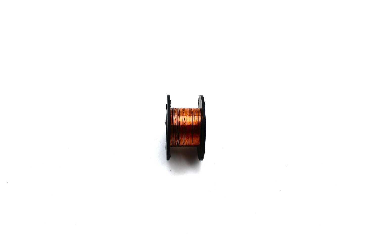
0.1 mm Copper Enamelled Repair Reel Wire
For PCB rework — repair broken traces or add supplemental high-current wiring over existing thin traces. Enamelled copper wire bonds well with solder.
Special Considerations: High Frequency and Differential Pairs
Skin effect at high frequency: At RF and high-frequency digital frequencies, current concentrates at the conductor surface (skin depth). At 100 MHz, skin depth in copper is about 6.6 µm — only the outer skin of the trace carries current. IPC-2221 DC current formulas do not account for this. For RF traces above a few MHz, trace impedance (characteristic impedance Z₀) becomes the primary design constraint, not current capacity.
Microstrip and stripline impedance: A 50 Ω microstrip trace on a standard 1.6 mm FR4 board with 1 oz copper (εr ≈ 4.4) has a width of approximately 3 mm. A 90 Ω differential pair (USB 2.0, for example) uses two traces approximately 0.2 mm wide with 0.2 mm spacing. These widths have nothing to do with current capacity — they are set by impedance requirements.
Length matching: For high-speed differential signals (USB, HDMI, DDR memory), trace lengths within a pair must match to within a few mils to maintain signal integrity. EDA tools like KiCad and Altium have interactive length tuning and impedance calculators built in.
Online Calculators and EDA Tool Integration
Rather than manually solving the IPC-2221 formula, use these trusted tools:
- PCB Trace Width Calculator by Sierra Circuits (sierracircuits.com) — one of the most accurate online tools
- KiCad PCB Calculator — built into KiCad under Tools → PCB Calculator; handles trace width, differential pairs, via current, and more
- EasyEDA Online Calculator — accessible directly in the EasyEDA browser interface
- Altium Designer’s rule-driven width constraints — define current rules per net class and Altium highlights violations in real-time during layout
Always double-check calculator results against the table above and your intuition. Calculators assume uniform temperature, standard FR4, and ambient conditions — real-world boards in enclosures or high-altitude locations may need additional derating.

6 Flexible Arms Soldering Station with Alligator Clips
Hold PCBs steady while soldering high-current traces. Six flexible arms and swivelling alligator clips keep your board and components in perfect position.
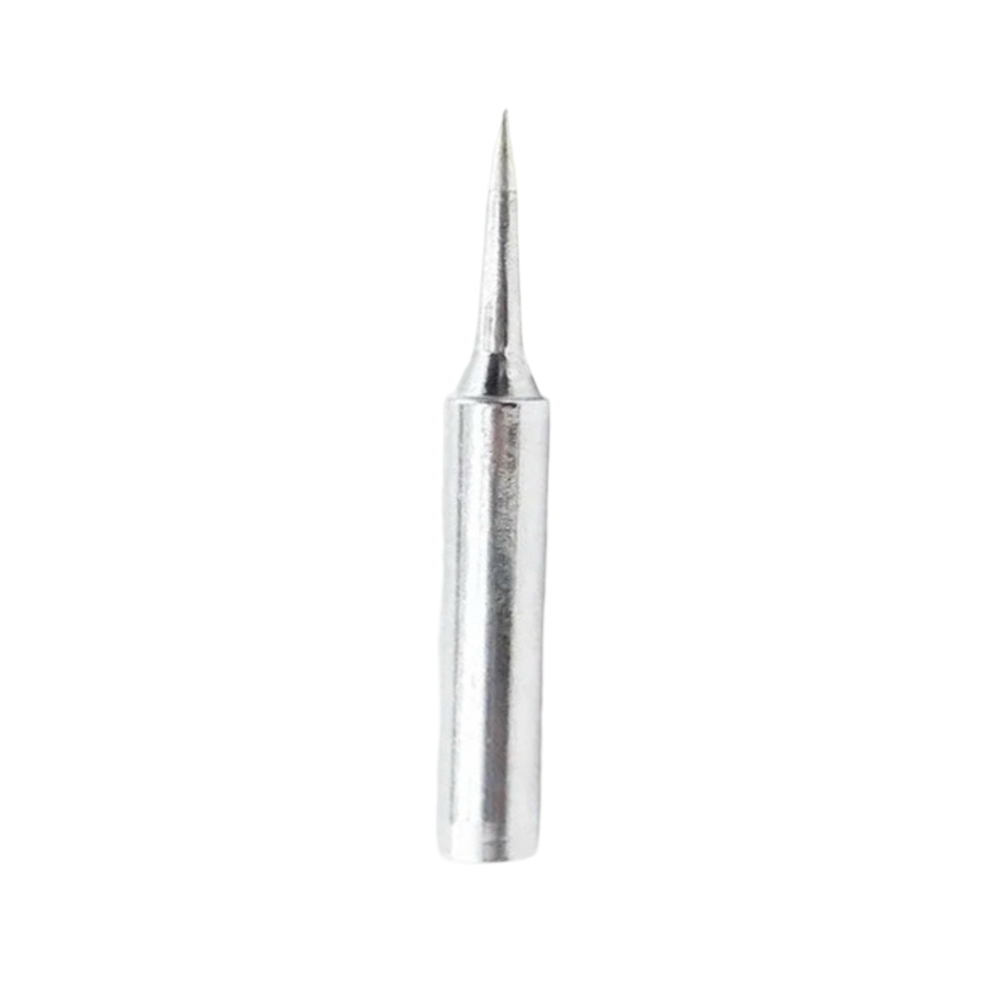
BAKON Soldering Iron Tip 900M-T-I
Precision I-type soldering tip for fine PCB work. Compatible with 900M-series stations — perfect for soldering fine traces and SMD components on prototype boards.
Frequently Asked Questions
What is 1 oz copper in mm?
1 oz/ft² copper (the most common PCB copper weight) equals approximately 35 µm or 0.035 mm thick. This corresponds to 1.4 mils in imperial units. Standard PCB manufacturers offer 0.5 oz, 1 oz, 2 oz, and 3 oz options. Heavier copper allows narrower traces for the same current but increases cost and minimum feature size.
How do I add extra current capacity without widening the trace?
Several approaches work: (1) Use heavier copper (2 oz doubles current capacity for the same width), (2) Run parallel traces on multiple layers connected by vias, (3) Solder a copper wire or bus bar on top of the trace, (4) Tin (pre-solder) the trace to increase its cross-section. All these are valid rework strategies when you discover a trace is undersized after fabrication.
Is 0.2 mm the minimum trace width I can use?
Most standard PCB manufacturers in India (PCBWay, JLCPCB, and local vendors) support a minimum trace width of 0.1–0.15 mm, but the practical minimum for reliable etching and handling is 0.2 mm. For signals carrying less than 100 mA, 0.2–0.3 mm is fine. Always check your manufacturer’s design rules before finalising the PCB.
Does the trace length affect current capacity?
Trace length does not affect the current carrying capacity (which is set by cross-sectional area and thermal rise), but it does affect voltage drop and resistance (R = ρ × L / A). A long, narrow power trace may have acceptable current capacity but unacceptable voltage drop for sensitive circuits. Always calculate both current capacity AND voltage drop for power traces.
What temperature rise should I design for in India?
India’s ambient temperature can reach 40–45°C in summer in northern and central regions. For equipment inside enclosures, add another 10–15°C for internal temperature rise. A conservative design targets a total maximum conductor temperature of 70–80°C, meaning ΔT = 25–35°C above a 45°C ambient. Always use the stricter temperature rise value for any safety-critical application.
Design With Confidence
Whether you are designing your first Arduino shield or a professional motor driver PCB, getting trace widths right is the foundation of a reliable circuit. Get your prototyping essentials — prototype boards, soldering tools, and passive components — from Zbotic with fast delivery across India.


Add comment